NCP4623 Просмотр технического описания (PDF) - ON Semiconductor
Номер в каталоге
Компоненты Описание
производитель
NCP4623 Datasheet PDF : 20 Pages
| |||
NCP4623
150 mA, Wide Input Voltage
Range, Low Dropout
Regulator
The NCP4623 is a CMOS Linear Voltage Regulator designed for
wide input voltage range. The maximum operating input voltage is up
to 24 V with a minimum voltage starting from 2 V. The Chip Enable
(CE) pin allows the device to lower standby current to 0.1 mA typ. The
NCP4623 features many protections for any current or thermal
sensitive devices with current fold−back protection, thermal shutdown
protection, and peak and short current protection. This device is
available in adjustable and fixed voltage output in 0.1 V steps. They
are available in very thin XDFN6 1.6x1.6x0.4 mm in size and the very
popular SOT23−5 and SOT89−5 packages. Please contact your local
sales office for additional output voltage options.
Features
• Maximum Operating Input Voltage: 24 V
• Output Voltage Range: 2.5 V to 12.0 V (available in 0.1 V steps)
2.5 V to 24.0 V (adjustable version)
• Output Voltage Accuracy: ±2.0%
• Supply Current: 5 mA
• Stable with Ceramic Capacitors: 1 mF or more
• Current Fold Back Protection
• Peak and Short Current Protection
• Thermal Shutdown Protection
• Available in XDFN6 1.6 x 1.6 mm, SOT23−5, SOT89−5 Packages
• These are Pb−Free Devices
Typical Applications
• Battery−powered Equipment
• Networking and Communication Equipment
• Cameras, DVRs, STB and Camcorders
• Home Appliances
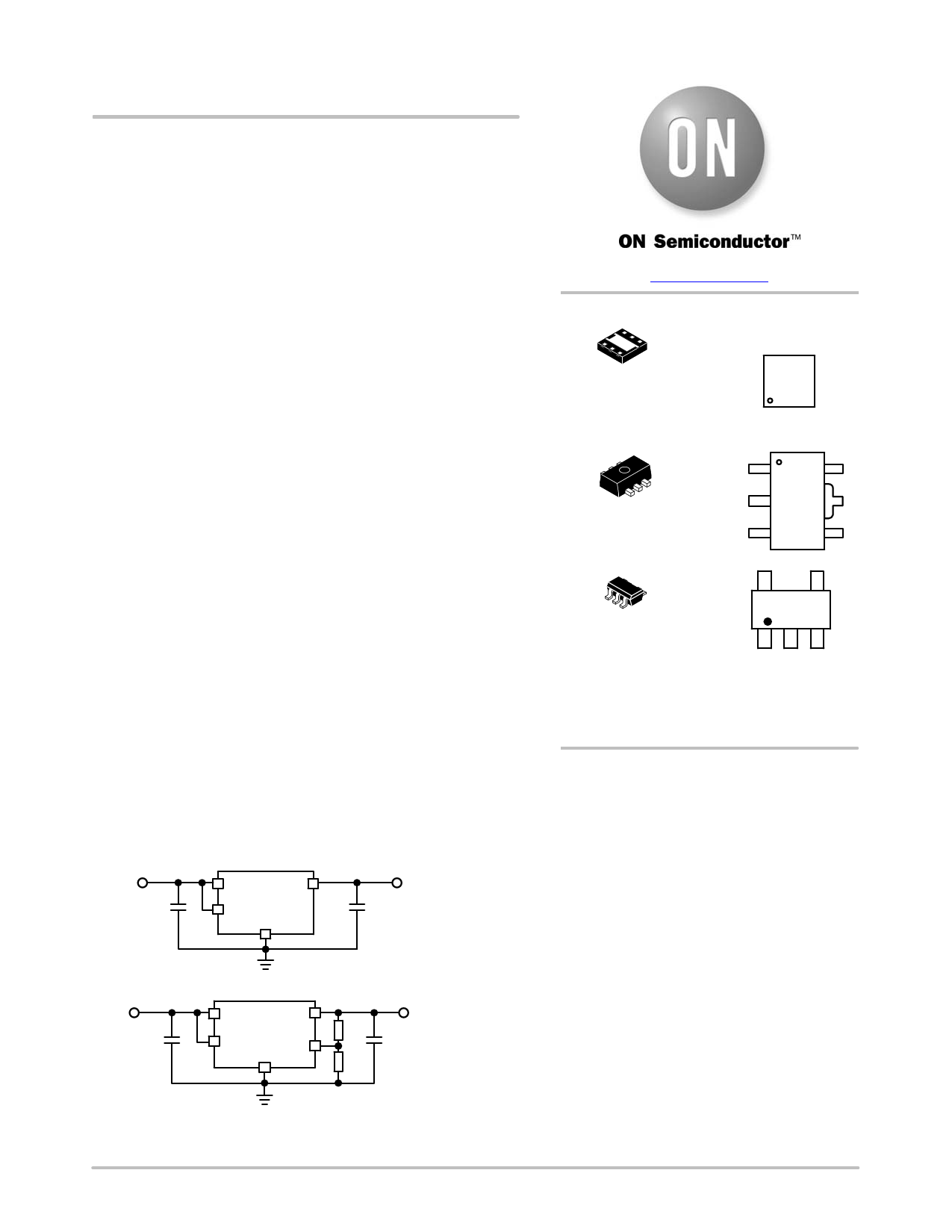
VIN
C1
100n
NCP4623x
VIN VOUT
CE
GND
VOUT
C2
100n
www.onsemi.com
MARKING
DIAGRAMS
XDFN6
CASE 711AC
XXX
XMM
1
SOT−89 5
CASE 528AB
1
XXX
XZZ
SOT−23−5
CASE 1212
XXXM
1
XXX, XXXX = Specific Device Code
M, MM = Date Code
ZZ
= Lot Code
ORDERING INFORMATION
See detailed ordering and shipping information in the package
dimensions section on page 17 of this data sheet.
VIN
C1
100n
NCP4623xADJ
VIN
VOUT
CE
ADJ
GND
VOUT
R1
C2
100n
R2
Figure 1. Typical Application Schematics
© Semiconductor Components Industries, LLC, 2016
1
January, 2016 − Rev. 4
Publication Order Number:
NCP4623/D
Share Link: 