NCP1246B65DR2G Просмотр технического описания (PDF) - ON Semiconductor
Номер в каталоге
Компоненты Описание
производитель
NCP1246B65DR2G Datasheet PDF : 38 Pages
| |||
NCP1246
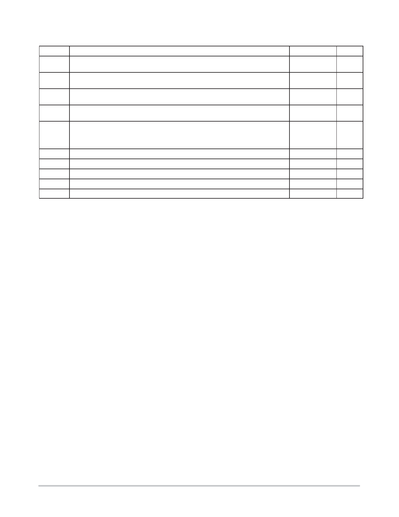
MAXIMUM RATINGS
Rating
Symbol
Value
Unit
DRV Maximum voltage on DRV pin
(pin 5) (DcïCurrent selfïlimited if operated within the allowed range) (Note 2)
–0.3 to 20
V
±1000 (peak)
mA
VCC
(pin 6)
HV
(pin 8)
VCCPower Supply voltage, VCC pin, continuous voltage
Power Supply voltage, VCC pin, continuous voltage (Note 2)
Maximum voltage on HV pin
(DcïCurrent selfïlimited if operated within the allowed range)
–0.3 to 28
V
±30 (peak)
mA
–0.3 to 500
V
±20
mA
Vmax
Maximum voltage on low power pins (except pin 5, pin 6 and pin 8)
(DcïCurrent selfïlimited if operated within the allowed range) (Note 2)
–0.3 to 10
V
±10 (peak)
mA
RqJïA
Thermal Resistance SOIC-7
Junction-to-Air, low conductivity PCB (Note 3)
Junction-to-Air, medium conductivity PCB (Note 4)
Junction-to-Air, high conductivity PCB (Note 5)
°C/W
162
147
115
RqJïC Thermal Resistance JunctionïtoïCase
TJMAX Operating Junction Temperature
TSTRGMAX Storage Temperature Range
ESD Capability, HBM model (All pins except HV)
73
ï40 to +150
ï60 to +150
> 2000
°C/W
°C
°C
V
ESD Capability, Machine Model (Note 1)
> 200
V
Stresses exceeding Maximum Ratings may damage the device. Maximum Ratings are stress ratings only. Functional operation above the
Recommended Operating Conditions is not implied. Extended exposure to stresses above the Recommended Operating Conditions may affect
device reliability.
1. This device series contains ESD protection and exceeds the following tests:
Human Body Model 2000 V per JEDEC standard JESD22, Method A114E
Machine Model Method 200 V per JEDEC standard JESD22, Method A115A
2. This device contains latch-up protection and exceeds 100 mA per JEDEC Standard JESD78.
3. As mounted on a 80 x 100 x 1.5 mm FR4 substrate with a single layer of 50 mm2 of 2 oz copper traces and heat spreading area. As specified
for a JEDEC 51-1 conductivity test PCB. Test conditions were under natural convection or zero air flow.
4. As mounted on a 80 x 100 x 1.5 mm FR4 substrate with a single layer of 100 mm2 of 2 oz copper traces and heat spreading area. As specified
for a JEDEC 51-2 conductivity test PCB. Test conditions were under natural convection or zero air flow.
5. As mounted on a 80 x 100 x 1.5 mm FR4 substrate with a single layer of 650 mm2 of 2 oz copper traces and heat spreading area. As specified
for a JEDEC 51-3 conductivity test PCB. Test conditions were under natural convection or zero air flow.
http://onsemi.com
4
Share Link: 