HI20201JCP Просмотр технического описания (PDF) - Intersil
Номер в каталоге
Компоненты Описание
производитель
HI20201JCP Datasheet PDF : 11 Pages
| |||
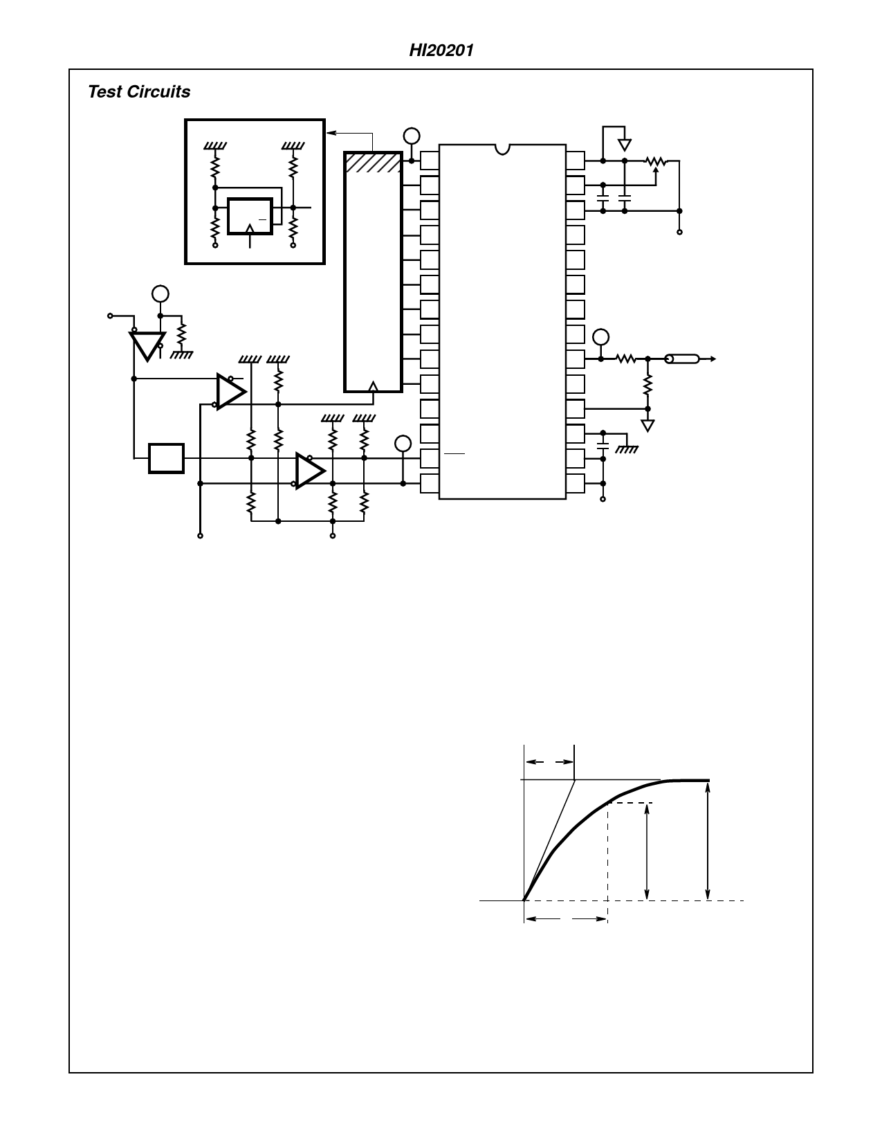
HI20201
Test Circuits (Continued)
-1.3V
1/6 HD100151
82
82
DQ
131
Q
131
TO PG
-5.2V CLKF -5.2V
50Ω
1
HD100116
82
1
470
DL
131
-1.3V
131
1
B
1 MSB
10kΩ
28
2
27
3
26
4
25
-5.2V
5
24
6
23
7
22
8
9
CLKF
10 LSB
11
21 C
39
50Ω
OUT 20
TO SCOPE
19
100
18
12
17
82 82 A
13 CLK
16
14 CLK
15
131 131
-5.2V
DL: Delay line
-5.2V
Capacitors are 0.047µF ceramic chip capacitors unless otherwise specified.
FIGURE 11. MAXIMUM CONVERSION RATE, RISE TIME, FALL TIME, PROPAGATION DELAY, SETUP TIME, HOLD TIME AND
SETTLING TIME CIRCUIT
Measuring Settling Time
Settling time is measured as follows. The relationship
between V and V0(FS) as shown in the D/A output waveform
in Figure 12 is expressed as
V = V0(FS) (1 - e-tτ).
The settling time for respective accuracy of 10, 9 and 8-bit is
specified as
V = 0.9995 V0(FS)
V = 0.999 V0(FS)
V = 0.999 V0(FS)
which results in the following:
tS
tS
=
=
7.60τ
6.93τ
for 10-bit,
for 9-bit, and
tS = 6.24τ for 8-bit,
Rise time (tr) and fall time (tf) are defined as the time interval
to slew from 10% to 90% of full scale voltage (V0(FS)):
V = 0.1 V0(FS)
V = 0.9 V0(FS)
and calculated as tr = tf = 2.20τ.
The settling time is obtained by combining these expressions:
tS = 3.45tr for 10-bit,
tS = 3.15tr for 9-bit, and
tS = 6.24tr for 8-bit
τ
V0(FS) = 1V
V
τ
FIGURE 12. D/A OUTPUT WAVEFORM
10-1205
Share Link: 