HI20201 Просмотр технического описания (PDF) - Intersil
Номер в каталоге
Компоненты Описание
производитель
HI20201 Datasheet PDF : 11 Pages
| |||
HI20201
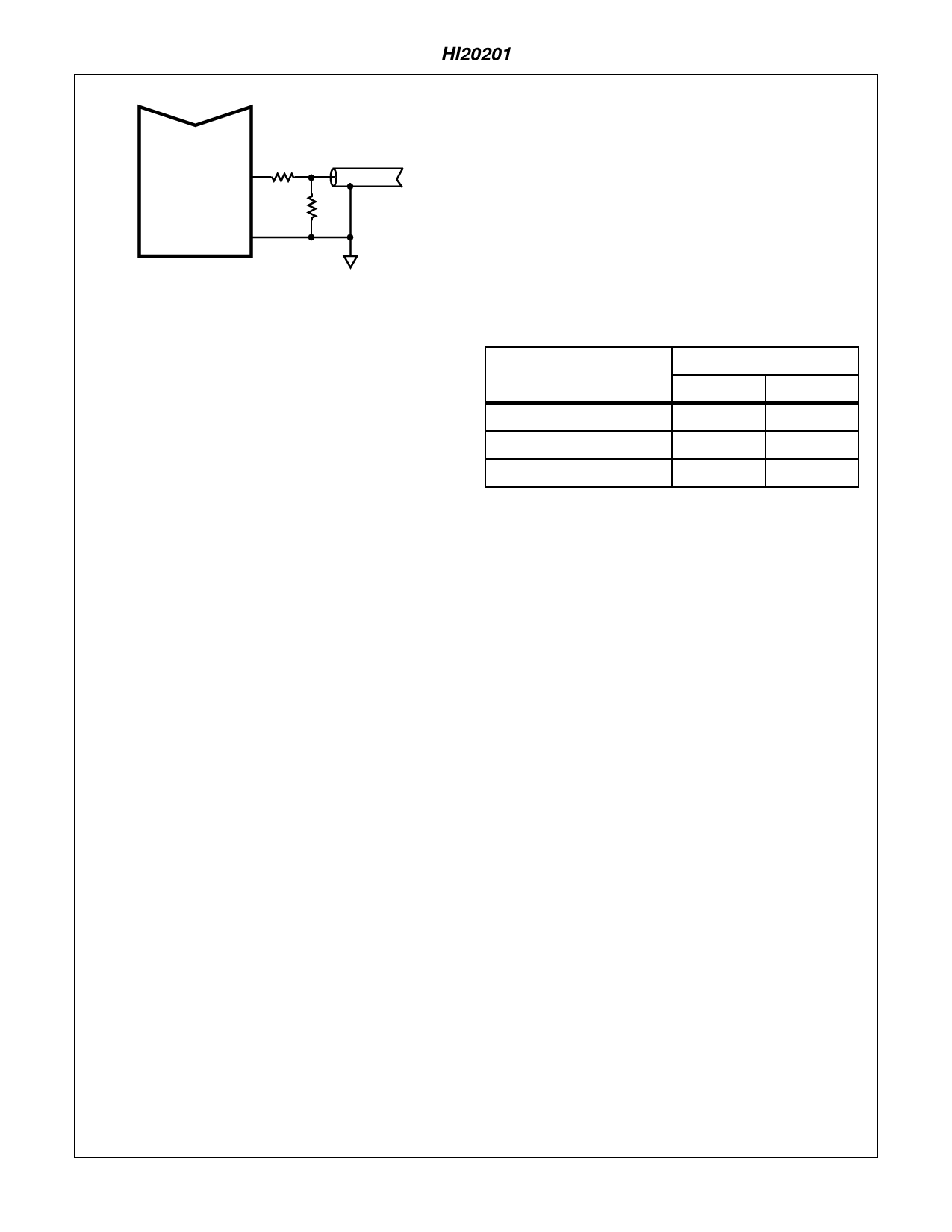
HI20201
39Ω
(20) IOUT
50Ω COAX CABLE
D/A OUT
100Ω
(18, 19, 21-25) NC
FIGURE 8. HI20201 DRIVING A 50Ω LOAD
Variable Attenuator Capability
The HI20201 can be used in a multiplying mode with a
variable frequency input on the VREF pin. In order for the
part to operate correctly a DC bias must be applied and the
incoming AC signal should be coupled to the VREF pin. See
Figure 13 for the application circuit. The user must first
adjust the DC reference voltage. The incoming signal must
be attenuated so as not to exceed the maximum (+1.4V) and
minimum (+0.5V) reference input. The typical output Small
Signal Bandwidth is 14MHz.
Integral Linearity
The Integral Linearity is measured using the End Point
method. In the End Point method the gain is adjusted. A line
is then established from the zero point to the end point or
Full Scale of the converter. All codes along the transfer curve
must fall within an error band of 1 LSB of the line. Figure 10
shows the linearity test circuit.
Differential Linearity
The Differential Linearity is the difference from the ideal step.
To guarantee monotonicity a maximum of 1 LSB differential
error is allowed. When more than 1 LSB is specified the con-
verter is considered to be missing codes. Figure 10 shows
the linearity test circuit.
Clock Phase Relationship
The HI20201 is designed to be operated at very high speed
(i.e., 160MHz). The clock lines should be driven with
ECL100K logic for full performance. Any external data
drivers and clock drivers should be terminated with 50Ω to
minimize reflections and ringing.
Internal Data Register
The HI20201 incorporates a data register as shown in the
Functional Block Diagram. This register is updated on the
rising edge of the CLK line. The state of the Complement bit
(COMPL) will determine the data coding. See Table 2.
TABLE 2. INPUT CODING TABLE
INPUT CODE
00 0000 0000
10 0000 0000
11 1111 1111
OUTPUT CODE
COMPL = 1 COMPL = 0
0
-1
-0.5
-0.5
-1
0
Thermal Considerations
The temperature coefficient of the full scale output voltage
and zero offset voltage depend on the load resistance con-
nected to IOUT. The larger the load resistor, the better (i.e.,
smaller) the temperature coefficient of the D/A. See Figure 3
in the performance curves section.
Noise Reduction
Digital switching noise must be minimized to guarantee system
specifications. Since 1 LSB corresponds to 1mV for 10-bit reso-
lution, care must be taken in the layout of a circuit board.
Separate ground planes should be used for DVSS and
AVSS. They should be connected back at the power supply.
Separate power planes should be used for DVEE and AVEE.
They should be decoupled with a 1µF tantalum capacitor
and a ceramic 0.047µF capacitor positioned as close to the
body of the IC as possible.
10-1203
Share Link: 