GLT41016-10E Просмотр технического описания (PDF) - G-Link Technology
Номер в каталоге
Компоненты Описание
производитель
GLT41016-10E Datasheet PDF : 12 Pages
| |||
GLT41016-10E
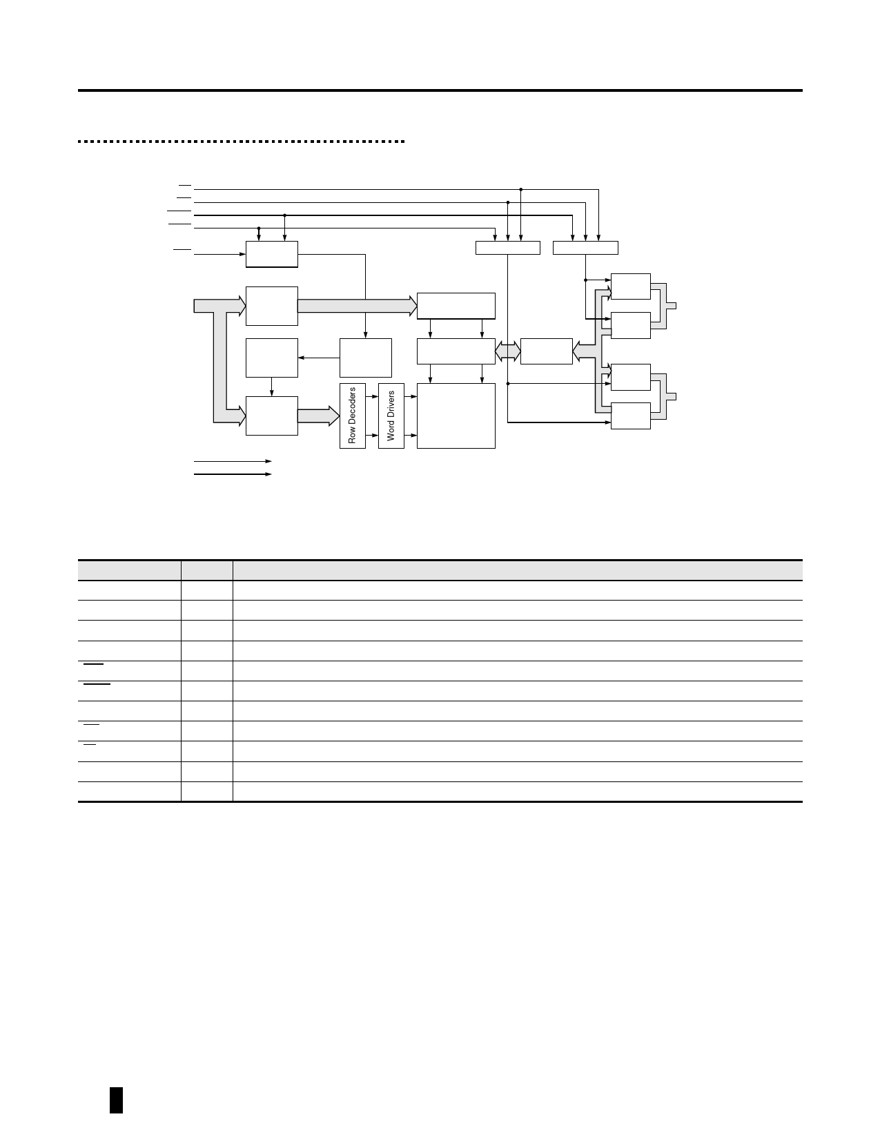
FUNCTIONAL BLOCK DIAGRAM
OE
WE
UCAS
LCAS
RAS
A[8:0]
Timing
Generator
Column
Address
Buffers
Internal
Address
Counter
Row
Address
Buffers
X[8:0]
Y[8:0]
Refresh
Control
Clock
I/O Controller
I/O Controller
Column Decoders
Sense Amps
I/O Selector
Memory Cells
Output
Buffer
Input
Buffer
Output
Buffer
Input
Buffer
VSS
VCC
Figure 1. GLT44016 - 256K X 16
Signal Descriptions [1]
Symbol
Type
Description
DI[15:0]
Input Data in.
DO[15:0]
Output Data out.
XRA[7:0]
Input Row address.
XCA[7:0]
Input Column address.
RAS
Input Row address strobe (active low).
CASH
Input Column address strobe, access DI/DO[15:8] (active low)
CASL
Input Column address strobe, access DI/DO[7:0] (active low)
WE
Input Write enable (active low).
OE
Input Output enable (active low).
VDD
Supply 3.3v voltage supply, 2 pairs double bond minimum
VSS
Supply Ground (voltage return), 2 pairs double bond minimum
1. On-chip power supply to the EmDRAM should be separated from the Logic portion.
DQ[7:0]
DQ[15:8]
2
G-LINK Technology
May 1997 (Rev. 1)
Share Link: 