MT90733 Просмотр технического описания (PDF) - Mitel Networks
Номер в каталоге
Компоненты Описание
производитель
MT90733 Datasheet PDF : 8 Pages
| |||
Advance Information
CMOS MT90733
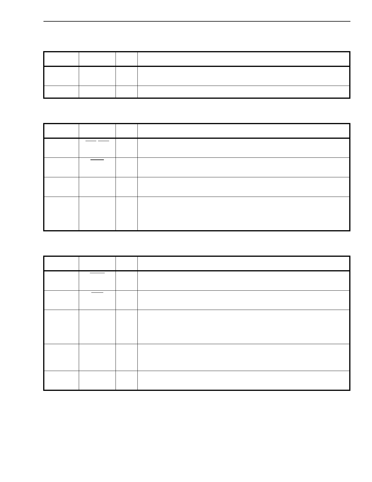
DS3 Transmit Line Side Interface
Pin #
Name I/O/P
Description
1
D3TC
O DS3 Transmit Clock. A 44.736 MHz clock that is derived from the transmit
clock (XCK) signal and is used for clocking out the line side DS3 data signal.
3
D3TD
O DS3 Transmit Data. DS3 line side serial transmit data.
Note: I = Input; O = Output; P = Power
Receive Terminal Side Interface
Pin #
Name I/O/P
Description
31
RFS/RFN O Receive Framing Pulse for Serial/Nibble Interface. The framing pulse is
synchronous with the first bit 1 in the DS3 frame or nibble 1175.
32
RCG
O Receive Clock Gap Signal. The active low gap signal is synchronous with
each overhead bit in the serial DS3 frame (first bit in the 85-bit group).
34
RCS/RCN O Receive Clock for Serial/Nibble Interface. Clock used for clocking out the
terminal side receive serial and nibble data.
39
RNIB3
O
40
RNIB2
41
RNIB1
42
RDS/RNIB0
Note: I = Input; O = Output; P = Power
Receive Nibble/Serial Interface. Nibble data is clocked out on positive transi-
tions of the nibble clock (RCN). Serial data is clocked out on negative transi-
tions of the receive clock (RCS).
Transmit Terminal Side Interface
Pin #
Name I/O/P
Description
2
XFNO
O Transmit Framing Pulse for Nibble Interface. An active low, one nibble clock
cycle wide (XCN) pulse that occurs during the second nibble time.
50
XFSI
I Transmit Framing Pulse for Serial Interface: A framing pulse input that must
be synchronous with bit 1 in the transmit serial data DS3 frame.
56
XDS/XNIB3 I Transmit Nibble/Serial Interface. Nibble data is clocked in on positive transi-
58
XNIB2
tions of the nibble clock (XCN). Serial data is clocked into the DS3F on posi-
59
XNIB1
tive transitions of the transmit clock (XCK).
60
XNIB0
62
XCK
I Transmit Clock. A 44.736 Mbit/s clock input with a stability of ±20 ppm and a
duty cycle of 50 ±10%. XCK provides the time base for the transmitter in the
DS3F.
66
XCN
O
Note: I = Input; O = Output; P = Power
Transmit Clock for Nibble Interface. Output clock signal derived from the
transmit clock (XCK).
5-25
Share Link: 