MT9074 Просмотр технического описания (PDF) - Mitel Networks
Номер в каталоге
Компоненты Описание
производитель
MT9074 Datasheet PDF : 122 Pages
| |||
Advance Information
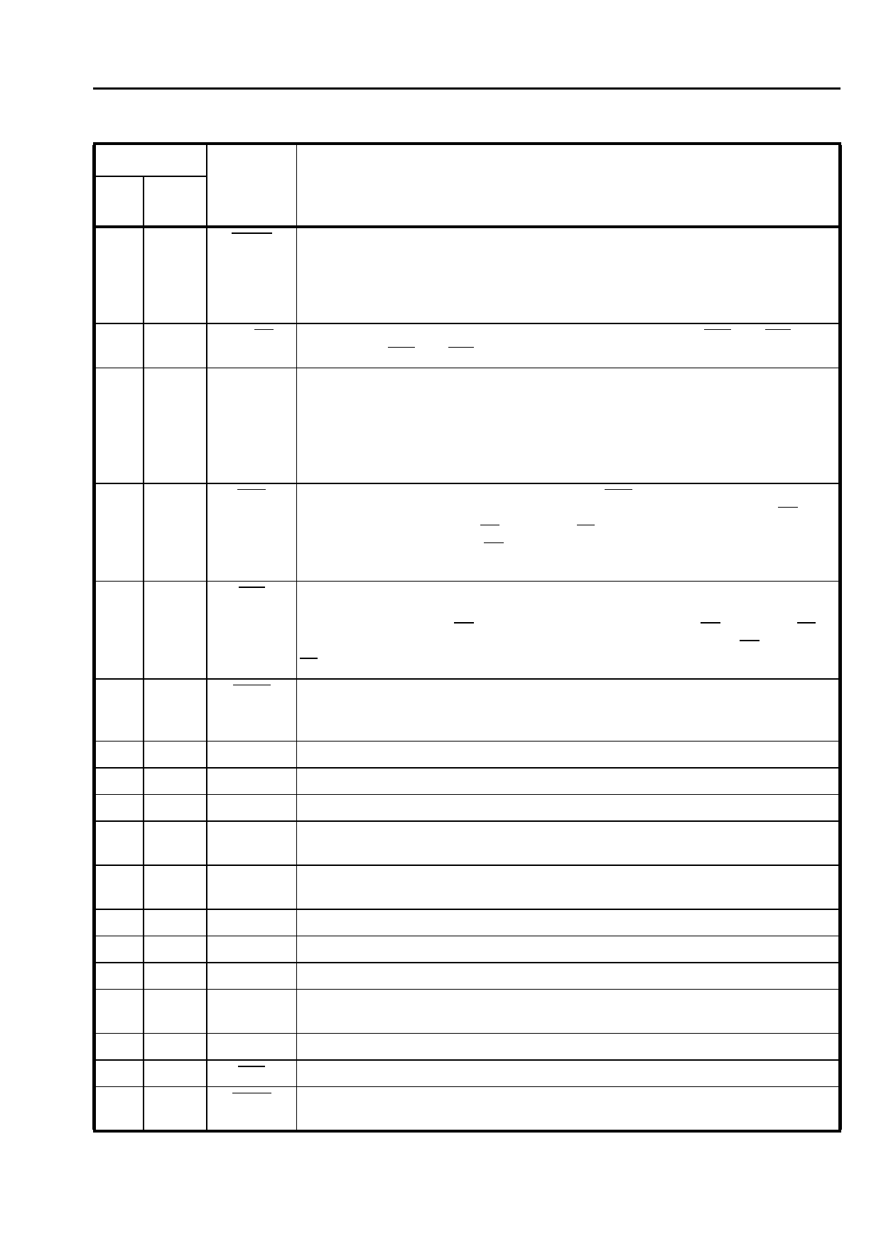
MT9074
Pin Description
Pin #
68 Pin 100 Pin
PLCC MQFP
Name
Description
42
23
RxMF
Receive Multiframe Boundary (Output). An output pulse delimiting the received
multiframe boundary. The next frame output on the data stream (DSTo) is basic
frame zero on the T1 or PCM 30 link. In E1 mode this receive multiframe signal
can be related to either the receive CRC multiframe (page 01H, address 17H, bit 6,
MFSEL=1) or the receive signalling multiframe (MFSEL=0).
43
24
BS/LS Bus/Line Synchronization Mode Selection (Input). If high, C4b and F0b will be
inputs; if low, C4b and F0b will be outputs.
44
32 E1.5o/C1.5o 2.048 MHz in E1 mode or 1.544MHz in T1 mode, Extracted Clock (Output).
If the internal L/U is enabled, this output is the clock extracted from the received
signal and used internally to clock in data received on RTIP and RRING. If the
internal LIU is disabled (digital framer mode), this output is a 1.544MHz clock
(T1) C1.5o or a 2.048 MHz clock C2o which clocks out the transmit digital data
TXA, TXB.
45
33
C4b 4.096 MHz System Clock (Input/Output). C4b is the clock for the ST-BUS
sections and transmit serial PCM data of the MT9074. In the free-run (S/FR=0) or
line synchronous mode (S/FR=1 and BS/LS=0) this signal is an output, while in
bus synchronous mode (S/FR=1) this signal is an input clock which is phase-
locked to the extracted clock (E1.5o).
46
34
F0b Frame Pulse (Input/Output). This is the ST-BUS frame synchronization signal,
which delimits the 32 channel frame of CSTi, CSTo, DSTi, DSTo and the PCM30
link. In the free-run (S/FR=0) or line synchronous mode (S/FR=1 and BS/LS=0)
this signal is an output, while in the line synchrounous mode (S/FR=1 and BS/
LS=0) this signal is an input.
47
35
RxFP
Receive Frame Pulse (Output). An 8kHz pulse signal, which is low for one
extracted clock period. This signal is synchronized to the receive DS1 or PCM 30
basic frame boundary.
48
36
IC
Internal Connection. Must be left open for normal operation.
49
37
50
38
51
39
VSS
VDD
VDDATx
Negative Power Supply (Input). Digital ground.
Positive Power Supply (Input). Digital supply (+5V ± 5%).
Transmit Analog Power Supply (Input). Analog supply for the LIU transmitter
(+5V ± 5% 10%)).
52
40
53
41
TTIP Transmit TIP and RING (Outputs). Differential outputs for the transmit DS1 line
TRING signal - must be transformer coupled (See Figure 5).
54
42
GNDATx Transmit Analog Ground (Input). Analog ground for the LIU transmitter.
55
43
Tdi IEEE 1149.1 Test Data Input. If not used, this pin should be pulled high.
56
44
Tdo IEEE 1149.1 Test Data Output. If not used, this pin should be left unconnected.
57
45
Tms
IEEE 1149.1 Test Mode Selection (Input). If not used, this pin should be pulled
high.
58
46
Tclk IEEE 1149.1 Test Clock Signal (Input). If not used, this pin should be pulled high.
59
47
Trst IEEE 1149.1 Reset Signal (Input). If not used, this pin should be held low.
60
48
TxAO Transmit All Ones (Input).High - TTIP, TRING will transmit data normally. Low -
TTIP, TRING will transmit an all ones signal.
5
Share Link: 