MT16VDDF6464H(2008) Просмотр технического описания (PDF) - Micron Technology
Номер в каталоге
Компоненты Описание
производитель
MT16VDDF6464H Datasheet PDF : 15 Pages
| |||
512MB, 1GB (x64, DR) 200-Pin DDR SODIMM
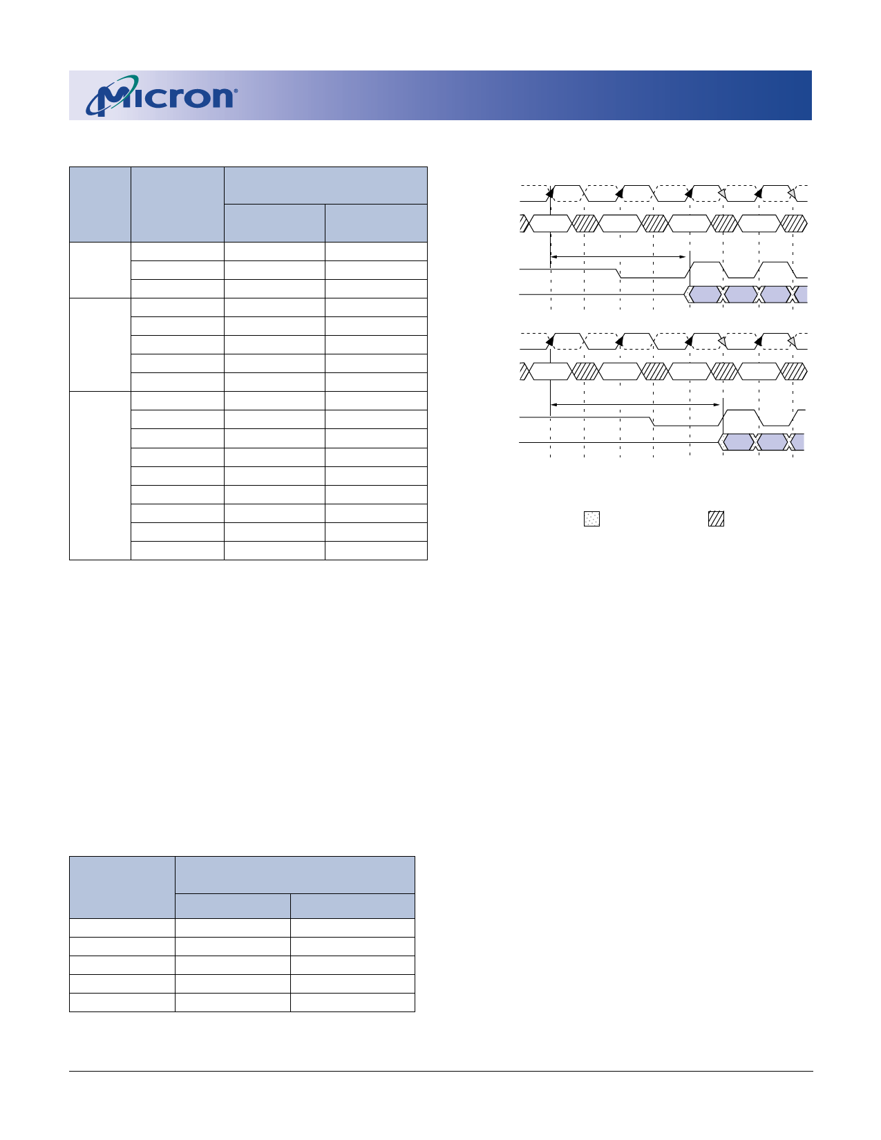
Electrical Specifications
IDD Specifications
Table 9:
IDD Specifications and Conditions – 512MB (Die Revison K)
Values are shown for the MT46V32M8 DDR SDRAM only and are computed from values specified in the
256Mb (32 Meg x 8) component data sheet
Parameter/Condition
Operating one bank active-precharge current: One device
bank; Active-precharge; tRC = tRC (MIN); tCK = tCK (MIN); DQ, DM,
and DQS inputs changing once per clock cycle; Address and control
inputs changing once every two clock cycles
Operating one bank active-read-precharge current: One device
bank; Active-read-precharge; BL = 4; tRC = tRC (MIN);
tCK = tCK (MIN); IOUT = 0mA; Address and control inputs changing
once per clock cycle
Precharge power-down standby current: All device banks idle;
Power-down mode; tCK = tCK (MIN); CKE = (LOW)
Idle standby current: CS# = HIGH; All device banks are idle;
tCK = tCK (MIN); CKE = HIGH; Address and other control inputs
changing once per clock cycle. VIN = VREF for DQ, DQS, and DM
Active power-down standby current: One device bank active;
Power-down mode; tCK = tCK (MIN); CKE = LOW
Active standby current: CS# = HIGH; CKE = HIGH; One device
bank active; tRC = tRAS (MAX); tCK = tCK (MIN); DQ, DM, and DQS
inputs changing twice per clock cycle; Address and other control
inputs changing once per clock cycle
Operating burst read current: BL = 2; Continuous burst reads;
One device bank active; Address and control inputs changing once
per clock cycle; tCK = tCK (MIN); IOUT = 0mA
Operating burst write current: BL = 2; Continuous burst writes;
One device bank active; Address and control inputs changing once
per clock cycle; tCK = tCK (MIN); DQ, DM, and DQS inputs changing
twice per clock cycle
Auto refresh burst current
tREFC = tRFC (MIN)
tREFC = 7.8125µs
Self refresh current: CKE ≤ 0.2V
Standard
Low power
Operating bank interleave read current: Four device bank
interleaving reads (BL = 4) with auto precharge;
tRC = (MIN) tRC allowed; tCK = tCK (MIN); Address and control
inputs change only during active READ or WRITE commands
Symbol
IDD01
IDD11
IDD2P2
IDD2F2
IDD3P2
IDD3N2
IDD4R1
IDD4W1
IDD52
IDD5A2
IDD62, 3
IDD6A2, 3
IDD71
-40B
832
992
64
800
560
960
1,472
1,472
2,560
96
64
32
2,352
-335
752
952
64
800
480
880
1,132
1,312
2,560
96
64
32
2,192
Units
mA
mA
mA
mA
mA
mA
mA
mA
mA
mA
mA
mA
mA
Notes:
1. Value calculated as one module rank in this operating condition; all other module ranks are
in IDD2P (CKE LOW) mode.
2. Value calculated reflects all module ranks in this operating condition.
3. The standard module guarantees IDD6 and the low-power module guarantees IDD6A.
PDF: 09005aef80a77a90/Source: 09005aef80a646bc
DDF16C64_128x64_L_H.fm - Rev. G 8/08 EN
10
Micron Technology, Inc., reserves the right to change products or specifications without notice.
©2003 Micron Technology, Inc. All rights reserved
Share Link: 