MSM5299C Просмотр технического описания (PDF) - Oki Electric Industry
Номер в каталоге
Компоненты Описание
производитель
MSM5299C Datasheet PDF : 11 Pages
| |||
¡ Semiconductor
MSM5299C
• O1 to O80
Display data output pins which correspond to the respective latch contents. One of V1, V3,
V4 and VEE is selected as a display driving voltage source based on the combination of the
latched data level and DF signal. (Refer to the Truth Table).
The outputs O1 to O80 are connected to the segment side of the LCD panel.
• DISP OFF
Input pin for controlling the outputs of O1 to O80. V1 level is output from O1 to O80 pins during
"L" level input. Refer to the Truth Table.
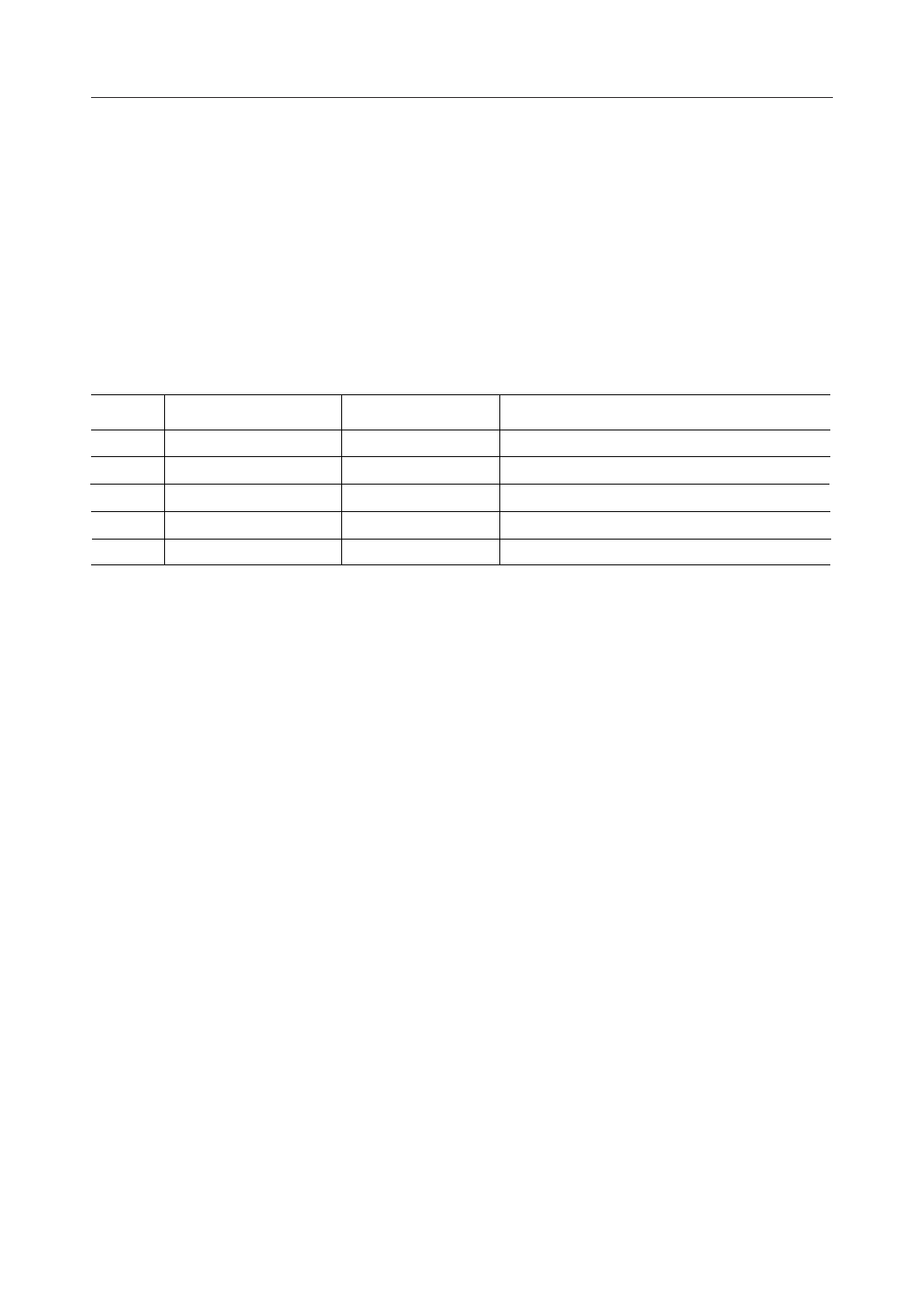
Truth Table
DF
Latched data
L
L
L
H
H
L
H
H
X
X
DISP OFF
H
H
H
H
L
Driver output level (O1-O80)
V3
V1
V4
VEE
V1
NOTES ON USE
Note the following when turning power on and off :
The LCD drivers of this IC require a high voltage. For this reason, if a high voltage is applied to
the LCD drivers with the logic power supply floating, excess current flows. This may damage
the IC. Be sure to carry out the follwing power-on and power-off sequences :
When turning power on :
First VDD ON, next VEE, V4, V3, V1 ON. Or both ON at the same time.
When turning power off :
First VEE, V4, V3, V1 OFF, next VDD OFF. Or both OFF at the same time.
9/11
Share Link: 