MSM5299A Просмотр технического описания (PDF) - Oki Electric Industry
Номер в каталоге
Компоненты Описание
производитель
MSM5299A Datasheet PDF : 11 Pages
| |||
¡ Semiconductor
MSM5299A
• D0, D1, D2, D3
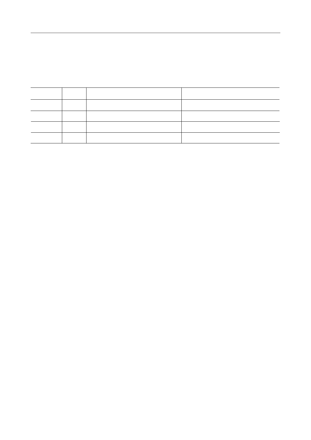
Display data input pins for 4 ¥ 20-bit shift register. The display data is clocked into the shift
register at the falling edge of the clock pulse. The combinations of D0 to D3 level, DF signal
level, display data output level and the display on the LCD panel are described on the table
below.
D0 to D3
DF
L
L
H
L
L
H
H
H
Display data output level
Nonselect level (V3)
Select level (V1)
Nonselect level (V4)
Select level (VEE)
Display on the LCD
OFF
ON
OFF
ON
• LOAD
The signal for latching the shift register contents is input to this pin. The display data stored
in the shift register is latched at the falling edge of the load pulse.
• DF
Synchronous signal input pin for alternate signal for LCD driving.
• VDD, VSS
Supply voltage pins, VDD should be 4.5 to 5.5V. VSS is a ground pin (VSS = 0V)
• V1, V3, V4, VEE
Bias supply voltage pin to drive the LCD. Use an external bias voltage supply for driving the
LCD.
8/11
Share Link: 