MAX3676E Просмотр технического описания (PDF) - Maxim Integrated
Номер в каталоге
Компоненты Описание
производитель
MAX3676E Datasheet PDF : 16 Pages
| |||
622Mbps, 3.3V Clock-Recovery and
Data-Retiming IC with Limiting Amplifier
LOL
VCC
6k
PHADJ+ PHADJ- FIL+ FIL-
DQ
SDO+
SDO-
PECL
DDI+
DDI-
PECL
INSEL
PHASE/FREQ
DETECTOR
ADI-
LIMITER
ADI+
42dB
1.23V
BIAS
OFFSET
CORRECTION
POWER
DETECT
Σ
FILTER
I
VCO
Q
622.08MHz
VCC
6k
SCLKO+
SCLKO-
PECL
MAX3676
OLC+ OLC-
CFILT RSSI INV
VTH
LOP
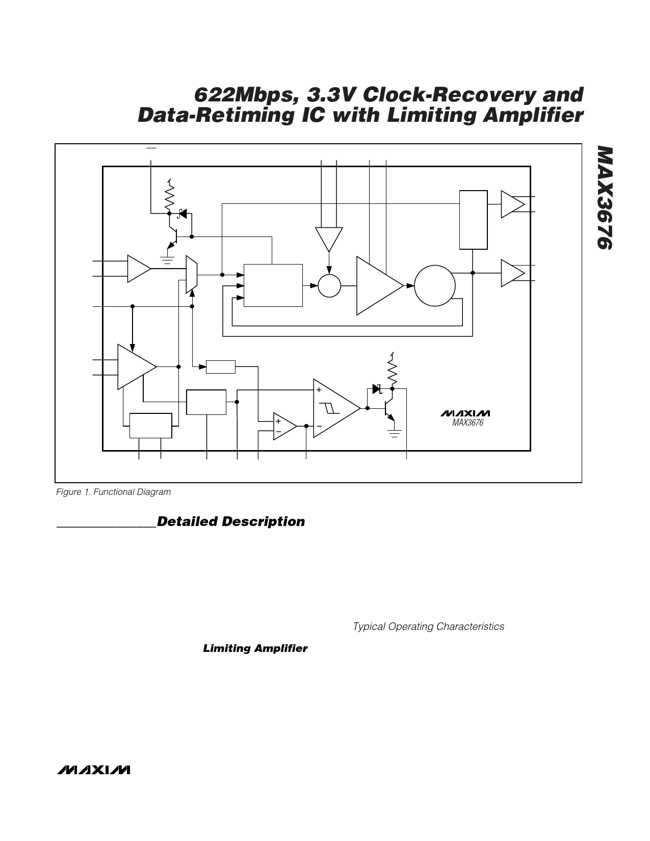
Figure 1. Functional Diagram
_______________Detailed Description
The block diagram in Figure 1 shows the MAX3676’s
architecture. It consists of a limiting-amplifier input
stage followed by a fully integrated clock/data-recovery
(CDR) block implemented with a PLL. The input stage
is selectable between a limiting amplifier or a simple
PECL input buffer. The limiting amplifier provides an
LOP monitor and an RSSI output. The PLL consists of a
phase/frequency detector (PFD), a loop filter amplifier,
and a voltage-controlled oscillator (VCO).
Limiting Amplifier
The MAX3676’s on-chip limiting amplifier accepts an
input signal level from 3.0mVp-p to 1.2Vp-p. The ampli-
fier consists of a cascade of gain stages that include
full-wave logarithmic detectors. The combined small-
signal gain is approximately 42dB, and the -3dB band-
width is 650MHz. Input-referred noise is typically
80µVRMS, providing excellent sensitivity for small-ampli-
tude data streams.
In addition to driving the CDR, the limiting amplifier pro-
vides both an RSSI output and an LOP monitor that
allow the user to program the threshold voltage. The
RSSI circuitry provides an output voltage that is linearly
proportional to the input power (in decibels) detected
between the ADI+ and ADI- input pins and is sensitive
enough to reliably detect signals as small as 2mVp-p
(see Typical Operating Characteristics).
Input DC offset reduces the accuracy of the power
detector; therefore, an integrated feedback loop is
included that automatically nulls the input offset of the
gain stage. The addition of this offset-correction loop
requires that the input signal be AC-coupled when
using the ADI+ and ADI- inputs.
Finally, for applications that do not require the limiting
amplifier, selecting the digital inputs conserves power
by turning off the postamplifier block.
_______________________________________________________________________________________ 7
Share Link: 