MPC7455 Просмотр технического описания (PDF) - Freescale Semiconductor
Номер в каталоге
Компоненты Описание
производитель
MPC7455 Datasheet PDF : 64 Pages
| |||
Electrical and Thermal Characteristics
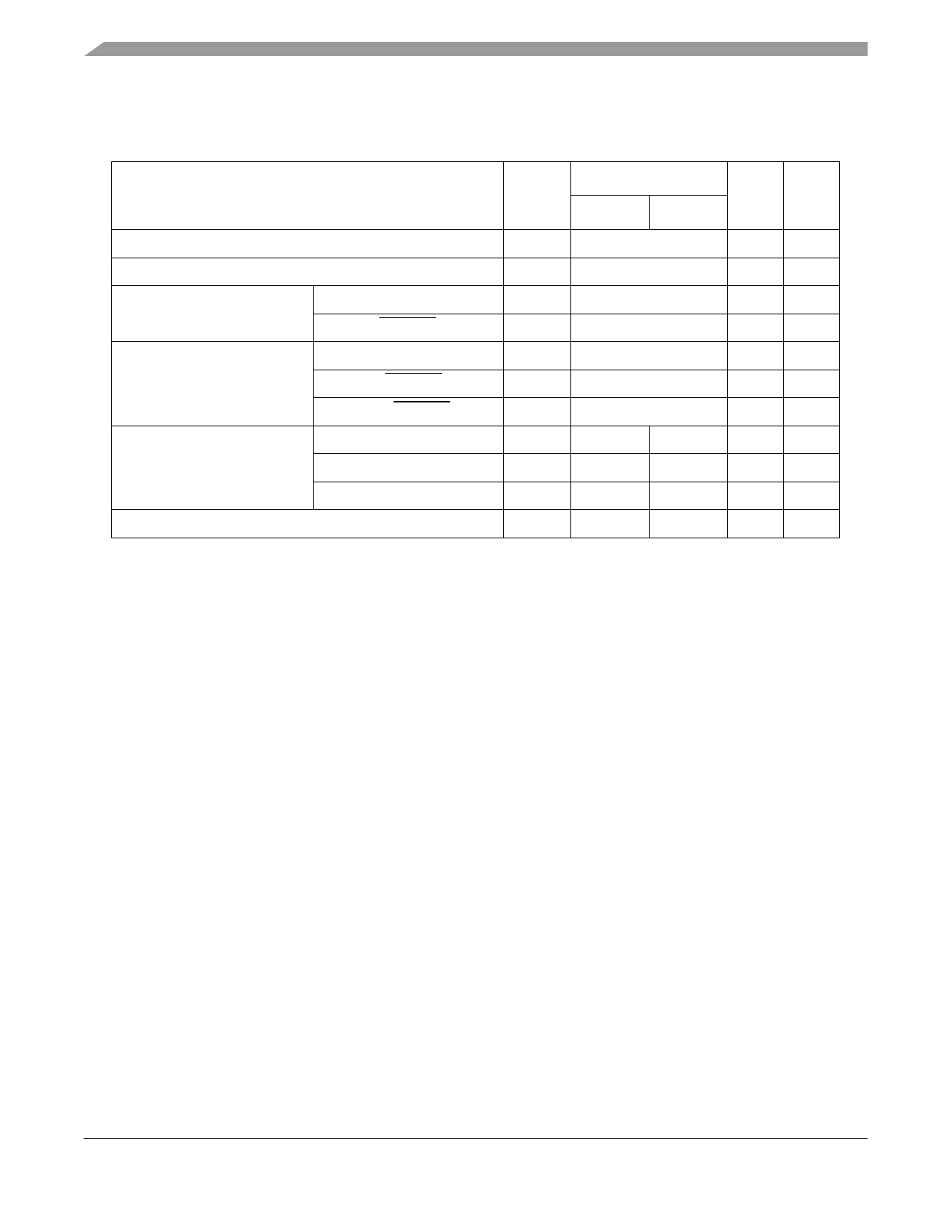
Table 4 provides the recommended operating conditions for the MPC7455.
Table 4. Recommended Operating Conditions 1
Characteristic
Recommended Value
Symbol
Unit Notes
Min
Max
Core supply voltage
VDD
1.3 V ± 50 mV
V
PLL supply voltage
AVDD
1.3 V ± 50 mV
V
2
Processor bus supply voltage BVSEL = 0
OVDD
1.8 V ± 5%
V
BVSEL = HRESET or OVDD OVDD
2.5 V ± 5%
V
L3 bus supply voltage
L3VSEL = 0
GVDD
1.8 V ± 5%
V
L3VSEL = HRESET or GVDD GVDD
2.5 V ± 5%
V
L3VSEL = ¬HRESET
GVDD
1.5 V ± 5%
V
Input voltage
Processor bus
Vin
GND
OVDD
V
L3 bus
Vin
GND
GVDD
V
JTAG signals
Vin
GND
OVDD
V
Die-junction temperature
Tj
0
105
°C
Notes:
1. These are the recommended and tested operating conditions. Proper device operation outside of these conditions
is not guaranteed.
2. This voltage is the input to the filter discussed in Section 9.2, “PLL Power Supply Filtering,” and not necessarily the
voltage at the AVDD pin which may be reduced from VDD by the filter.
MPC7455 RISC Microprocessor Hardware Specifications, Rev. 4.1
12
Freescale Semiconductor
Share Link: 