2N7002DW Просмотр технического описания (PDF) - Diodes Incorporated.
Номер в каталоге
Компоненты Описание
производитель
2N7002DW Datasheet PDF : 5 Pages
| |||
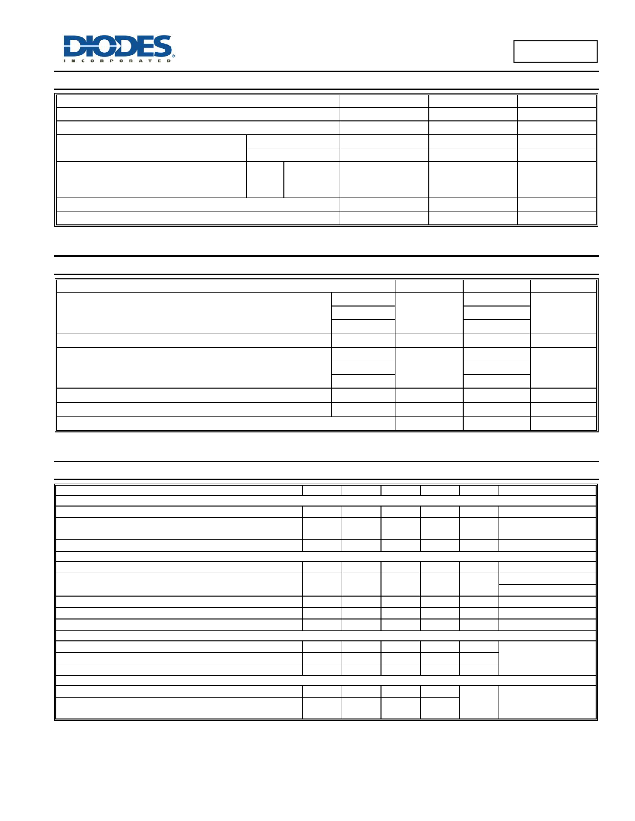
Maximum Ratings (@TA = +25°C, unless otherwise specified.)
Characteristic
Drain-Source Voltage
Drain-Gate Voltage RGS 1.0M
Gate-Source Voltage
Continuous Drain Current (Note 8) VGS = 5V
Steady
State
Maximum Continuous Body Diode Forward Current (Note 8)
Pulsed Drain Current (10µs Pulse, Duty Cycle = 1%)
Continuous
Pulsed
TA = +25C
TA = +70C
TA = +100C
Symbol
VDSS
VDGR
VGSS
VGSS
ID
IS
IDM
2N7002DW
Value
Unit
60
V
60
V
±20
V
±40
V
0.23
0.18
A
0.14
0.53
A
0.8
A
Thermal Characteristics (@TA = +25°C, unless otherwise specified.)
Characteristic
Total Power Dissipation (Note 7)
Thermal Resistance, Junction to Ambient (Note 7)
Total Power Dissipation (Note 8)
Thermal Resistance, Junction to Ambient (Note 8)
Thermal Resistance, Junction to Case (Note 8)
Operating and Storage Temperature Range
TA = +25°C
TA = +70°C
TA = +100°C
Steady State
TA = +25°C
TA = +70°C
TA = +100°C
Steady State
Steady State
Symbol
PD
RJA
PD
RJA
RJC
TJ, TSTG
Value
0.31
0.2
0.12
410
0.4
0.25
0.15
318
135
-55 to +150
Unit
W
°C/W
W
°C/W
°C/W
°C
Electrical Characteristics (@TA = +25°C, unless otherwise specified.)
Characteristic
Symbol Min
OFF CHARACTERISTICS (Note 9)
Drain-Source Breakdown Voltage
BVDSS
60
Zero Gate Voltage Drain Current
@ TC = +25°C
@ TC = +125°C
IDSS
Gate-Body Leakage
ON CHARACTERISTICS (Note 9)
IGSS
Gate Threshold Voltage
VGS(TH)
1.0
Static Drain-Source On-Resistance
@ TJ = +25°C
@ TJ = +125°C
RDS(ON)
On-State Drain Current
ID(ON)
0.5
Forward Transconductance
gFS
80
Diode Forward Voltage
DYNAMIC CHARACTERISTICS (Note 10)
VSD
Input Capacitance
Ciss
Output Capacitance
Coss
Reverse Transfer Capacitance
SWITCHING CHARACTERISTICS (Note 10)
Crss
Turn-On Delay Time
tD(ON)
Turn-Off Delay Time
tD(OFF)
Typ
70
3.2
4.4
1.0
0.78
22
11
2.0
7.0
11.0
Max
1.0
500
±10
2.0
7.5
13.5
1.5
50
25
5.0
20
20
Unit
V
µA
nA
V
A
mS
V
pF
pF
pF
ns
Notes:
7. Device mounted on FR-4 substrate PC board, 2oz copper, with minimum recommended pad layout.
8. Device mounted on FR-4 substrate PC board, 2oz copper, with thermal vias to bottom layer 1inch square copper plate.
9. Short duration pulse test used to minimize self-heating effect.
10. Guaranteed by design. Not subject to product testing.
Test Condition
VGS = 0V, ID = 10µA
VDS = 60V, VGS = 0V
VGS = ±20V, VDS = 0V
VDS = VGS, ID = 250µA
VGS = 5.0V, ID = 0.05A
VGS = 10V, ID = 0.5A
VGS = 10V, VDS = 7.5V
VDS =10V, ID = 0.2A
VGS = 0V, IS = 115mA
VDS = 25V, VGS = 0V
f = 1.0MHz
VDD = 30V, ID = 0.2A,
RL = 150, VGEN = 10V,
RGEN = 25
2N7002DW
Document number: DS30120 Rev. 17 - 2
2 of 5
www.diodes.com
December 2017
© Diodes Incorporated
Share Link: 