MOC8111 Просмотр технического описания (PDF) - Vishay Semiconductors
Номер в каталоге
Компоненты Описание
производитель
MOC8111 Datasheet PDF : 5 Pages
| |||
MOC8111/MOC8112
Vishay Semiconductors Optocoupler, Phototransistor Output,
No Base Connection
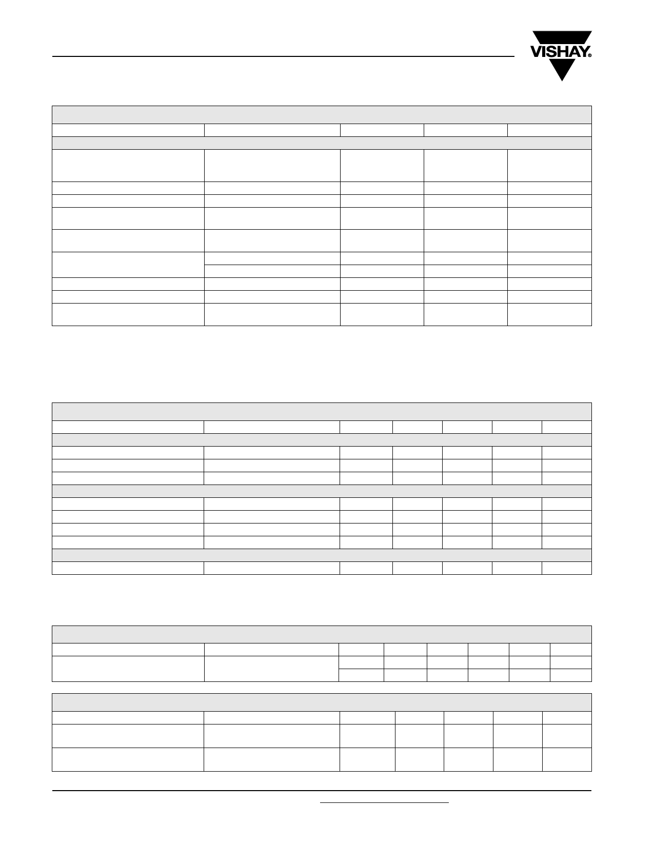
ABSOLUTE MAXIMUM RATINGS (1)
PARAMETER
COUPLER
Isolation test voltage between emitter
and detector refer to standard climate
23/50 DIN 50014
Creepage distance
Clearance distance
Isolation thickness between
emitter and detector
Comparative tracking index per
DIN IEC 112/VDE 0303, part 1
Isolation resistance
Storage temperature range
Ambient temperature range
Soldering temperature (2)
TEST CONDITION
VIO = 500 V, Tamb = 25 °C
VIO = 500 V, Tamb = 100 °C
max. 10 s, dip soldering distance
to seating plane ≥ 1.5 mm
SYMBOL
VISO
CTI
RIO
RIO
Tstg
Tamb
Tsld
VALUE
5300
≥7
≥7
≥4
175
1012
1011
- 55 to + 150
- 55 to + 100
260
UNIT
VRMS
mm
mm
mm
Ω
Ω
°C
°C
°C
Notes
(1) Tamb = 25 °C, unless otherwise specified.
Stresses in excess of the absolute maximum ratings can cause permanent damage to the device. Functional operation of the device is not
implied at these or any other conditions in excess of those given in the operational sections of this document. Exposure to absolute maximum
ratings for extended periods of the time can adversely affect reliability.
(2) Refer to reflow profile for soldering conditions for surface mounted devices (SMD). Refer to wave profile for soldering conditions for through
hole devices (DIP).
ELECTRICAL CHARACTERISTICS
PARAMETER
TEST CONDITION
SYMBOL
MIN.
TYP.
MAX.
UNIT
INPUT
Forward voltage
Reverse leakage current
Junction capacitance
OUTPUT
IF = 10 mA
VF
VR = 6.0 V
IR
V = 0 V, f = 1.0 MHz
Cj
1.15
1.5
V
0.05
10
µA
25
pF
Collector emitter breakdown voltage
IC = 1.0 µA
BVCEO
30
V
Collector emitter leakage current
VCE = 10 V
ICEO
1.0
50
nA
Emitter collector breakdown voltage
IE = 10 µA
BVECO
7.0
V
Collector emitter capacitance
VCE = 0 V, f = 1.0 MHz
CCE
7.0
pF
COUPLER
Collector saturation voltage
IC = 500 µA, IF = 10 mA
VCEsat
0.15
0.4
V
Note
Tamb = 25 °C, unless otherwise specified.
Minimum and maximum values are testing requirements. Typical values are characteristics of the device and are the result of engineering
evaluation. Typical values are for information only and are not part of the testing requirements.
CURRENT TRANSFER RATIO
PARAMETER
TEST CONDITION
Current transfer ratio
IF = 10 mA, VCE = 10 V
PART SYMBOL
MOC8111 CTR
MOC8112 CTR
MIN.
20
50
TYP.
MAX.
UNIT
%
%
SWITCHING CHARACTERISTICS
PARAMETER
Turn-on time
Turn-off time
TEST CONDITION
VCC = 10 V, RL = 100 Ω
IC = 2.0 mA, see figure 1
VCC = 10 V, RL = 100 Ω
IC = 2.0 mA, see figure 1
SYMBOL
ton
toff
MIN.
TYP.
7.5
5.7
MAX.
20
20
UNIT
µs
µs
www.vishay.com
2
For technical questions, contact: optocoupler.answers@vishay.com
Document Number: 83661
Rev. 1.5, 11-Jan-08
Share Link: 