MOC8101-X009(2008) Просмотр технического описания (PDF) - Vishay Semiconductors
Номер в каталоге
Компоненты Описание
производитель
MOC8101-X009 Datasheet PDF : 7 Pages
| |||
MOC8101/MOC8102/MOC8103/MOC8104/MOC8105
Vishay Semiconductors Optocoupler, Phototransistor Output,
No Base Connection
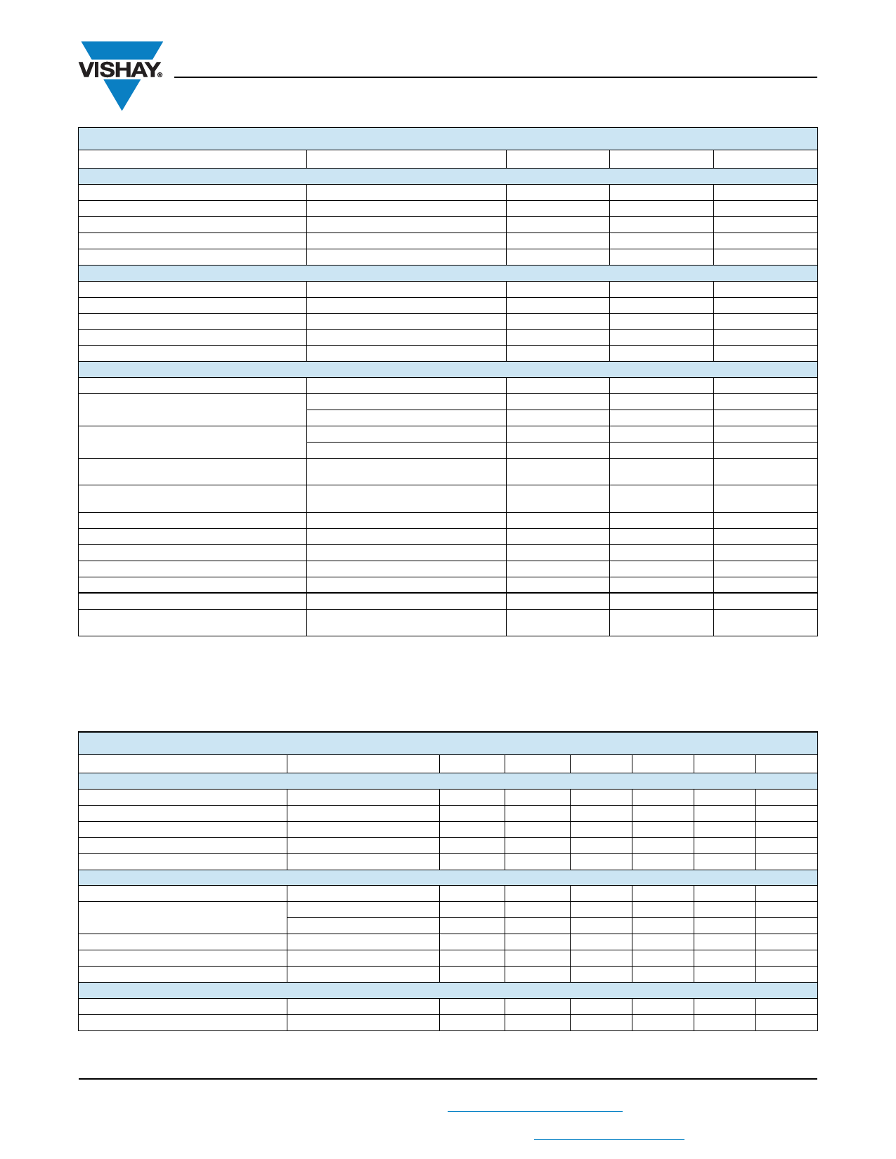
ABSOLUTE MAXIMUM RATINGS (1)
PARAMETER
INPUT
Reverse voltage
Forward continuous current
Surge forward current
Power dissipation
Derate linearly from 25°C
OUTPUT
Collector emitter breakdown voltage
Emitter collector breakdown voltage
Collector current
Derate linearly from 25°C
Power dissipation
COUPLER
Isolation test voltage
Creepage distance
Clearance distance
Isolation thickness between
emitter and detector
Comparative tracking index per
DIN IEC 112/VDE 0303, part 1
Isolation resistance
Derate linearly from 25 °C
Total power dissipation
Storage temperature
Operating temperature
Junction temperature
Soldering temperature (2)
TEST CONDITION
t ≤ 10 µs
VIO = 500 V
max. 10 s, dip soldering:
distance to seating plane
≥ 1.5 mm
SYMBOL
VR
IF
IFSM
Pdiss
BVCEO
BVECO
IC
Pdiss
VISO
CTI
RIO
Ptot
Tstg
Tamb
Tj
Tsld
VALUE
6.0
60
2.5
100
1.33
30
7.0
50
2.0
150
5300
≥ 7.0
≥ 7.0
≥ 0.4
175
1012
3.33
250
- 55 to + 150
- 55 to + 100
100
260
UNIT
V
mA
A
mW
mW/°C
V
V
mA
mW/°C
mW
VRMS
mm
mm
mm
Ω
mW/°C
mW
°C
°C
°C
°C
Notes
(1) Tamb = 25 °C, unless otherwise specified.
Stresses in excess of the absolute maximum ratings can cause permanent damage to the device. Functional operation of the device is not
implied at these or any other conditions in excess of those given in the operational sections of this document. Exposure to absolute maximum
ratings for extended periods of the time can adversely affect reliability.
(2) Refer to reflow profile for soldering conditions for surface mounted devices (SMD). Refer to wave profile for soldering conditions for through
hole devices (DIP).
ELECTRICAL CHARACTERISTICS
PARAMETER
INPUT
Forward voltage
Breakdown voltage
Reverse current
Capacitance
Thermal resistance
OUTPUT
Collector emitter capacitance
Collector emitter dark current
Collector emitter breakdown voltage
Emitter collector breakdown voltage
Thermal resistance
TEST CONDITION
PART SYMBOL
IF = 10 mA
IR = 10 µA
VR = 6.0 V
VR = 0 V, f = 1.0 MHz
VF
VBR
IR
CO
Rthja
VCE = 5.0 V, f = 1.0 MHz
VCE = 10 V, Tamp = 25 °C
VCE = 10 V, Tamp = 100 °C
IC = 1.0 mA
IE = 100 μA
MOC8101
MOC8102
CCE
ICEO1
ICEO1
BVCEO
BVECO
Rthja
MIN.
6.0
30
7.0
TYP.
1.25
0.01
25
750
5.2
1.0
1.0
500
MAX.
1.5
10
50
UNIT
V
V
µA
pF
K/W
pF
nA
µA
V
V
K/W
www.vishay.com
2
For technical questions, contact: optocoupler.answers@vishay.com
Document Number: 83660
Rev. 1.5, 11-Jan-08
Share Link: 