AD7818AR Просмотр технического описания (PDF) - Analog Devices
Номер в каталоге
Компоненты Описание
производитель
AD7818AR Datasheet PDF : 20 Pages
| |||
Pin
Mnemonic
1
CONVST
2
OTI
3
4 (AD7818)
GND
VIN
4 (AD7816)
REFIN
5
VDD
6
DIN/OUT
7
SCLK
8
RD/WR
AD7816/AD7817/AD7818
AD7816 AND AD7818 PIN FUNCTION DESCRIPTIONS
Description
Logic Input Signal. The convert start signal initiates a 10-bit analog-to-digital conversion on the
falling edge of the this signal. The falling edge of this signal places the track/hold in hold mode.
The track/hold goes into track mode again at the end of the conversion. The state of the
CONVST signal is checked at the end of a conversion. If it is logic low, the AD7816 and
AD7818 will power down—see Operating Mode section of the data sheet.
Logic Output. The Overtemperature Indicator (OTI) is set logic low if the result of a conversion
on Channel 0 (Temperature Sensor) is greater that an 8-bit word in the Overtemperature Register
(OTR). The signal is reset at the end of a serial read operation, i.e., a rising RD/WR edge.
Analog and Digital Ground.
Analog Input Channel. The input channel is single-ended with respect to GND. The input
channel can convert voltage signals in the range 0 V to 2.5 V. The input channel is selected by
writing to the Address Register of the AD7818—see Control Byte section.
Reference Input. An external 2.5 V reference can be connected to the AD7816 at this pin. To
enable the on-chip reference the REFIN pin should be tied to AGND. If an external reference is
connected to the AD7816, the internal reference will shut down.
Positive supply voltage, 2.7 V to 5.5 V.
Logic Input and Output. Serial data is clocked in and out of the AD7816/AD7818 at this pin.
Clock Input for the Serial Port. The serial clock is used to clock data into and out of the
AD7816/AD7818. Data is clocked out on the falling edge and clocked in on the rising edge.
Logic Input. The read/write signal is used to indicate to the AD7816 and AD7818 whether
the next data transfer operation is a read or a write. The RD/WR should be set logic high for a
read operation and logic low for a write.
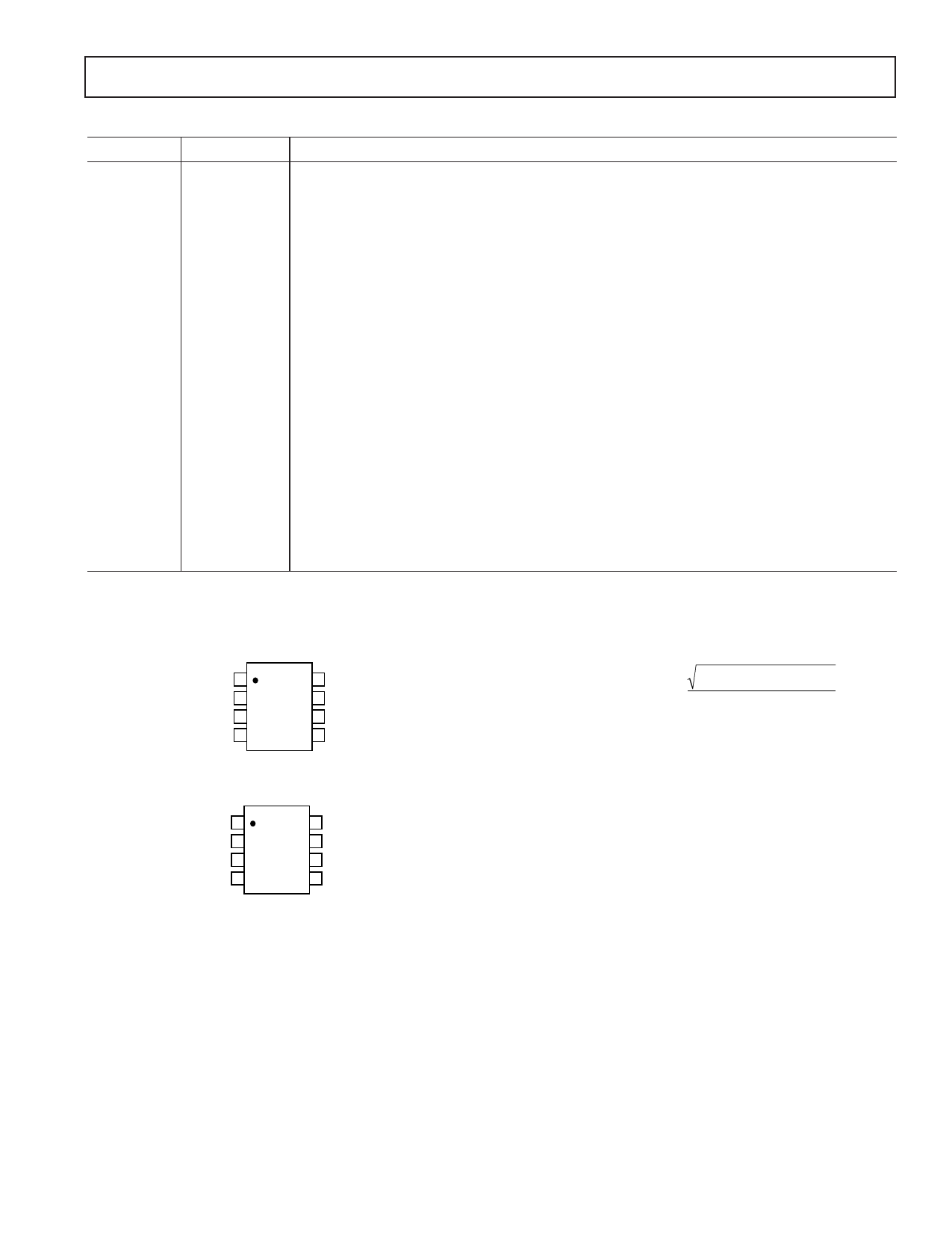
PIN CONFIGURATIONS
SOIC/MSOP (AD7816)
CONVST 1
8 RD/WR
OTI 2 AD7816 7 SCLK
TOP VIEW
GND 3 (Not to Scale) 6 DIN/OUT
REFIN 4
5 VDD
SOIC/MSOP (AD7818)
CONVST 1
8 RD/WR
OTI 2 AD7818 7 SCLK
TOP VIEW
GND 3 (Not to Scale) 6 DIN/OUT
VIN 4
5 VDD
TERMINOLOGY
Signal-to-(Noise + Distortion) Ratio
This is the measured ratio of signal-to-(noise + distortion) at the
output of the A/D converter. The signal is the rms amplitude of
the fundamental. Noise is the rms sum of all nonfundamental
signals up to half the sampling frequency (fS/2), excluding dc.
The ratio is dependent upon the number of quantization levels in
the digitization process; the more levels, the smaller the quantiza-
tion noise. The theoretical signal-to-(noise + distortion) ratio for
an ideal N-bit converter with a sine wave input is given by:
Signal-to-(Noise + Distortion) = (6.02 N + 1.76) dB
Thus for a 10-bit converter, this is 62 dB.
Total Harmonic Distortion
Total harmonic distortion (THD) is the ratio of the rms sum of
harmonics to the fundamental. For the AD7891 it is defined as:
THD (dB) = 20 log V22 +V32 +V42 +V52 +V62
V1
where V1 is the rms amplitude of the fundamental and V2, V3,
V4, V5, and V6 are the rms amplitudes of the second through the
sixth harmonics.
Peak Harmonic or Spurious Noise
Peak harmonic or spurious noise is defined as the ratio of the
rms value of the next largest component in the ADC output
spectrum (up to fS/2 and excluding dc) to the rms value of the
fundamental. Normally, the value of this specification is deter-
mined by the largest harmonic in the spectrum, but for parts
where the harmonics are buried in the noise floor, it will be a
noise peak.
Intermodulation Distortion
With inputs consisting of sine waves at two frequencies, fa and
fb, any active device with nonlinearities will create distortion
products at sum and difference frequencies of mfa Ϯ nfb where
m, n = 0, 1, 2, 3, etc. Intermodulation terms are those for which
neither m nor n are equal to zero. For example, the second
order terms include (fa + fb) and (fa – fb), while the third order
terms include (2fa + fb), (2fa – fb), (fa + 2fb) and (fa – 2fb).
REV. C
–9–
Share Link: 