MM1294 Просмотр технического описания (PDF) - Mitsumi
Номер в каталоге
Компоненты Описание
производитель
MM1294 Datasheet PDF : 6 Pages
| |||
MITSUMI
Protection of Lithium Ion Batteries (four cells in series) MM1294
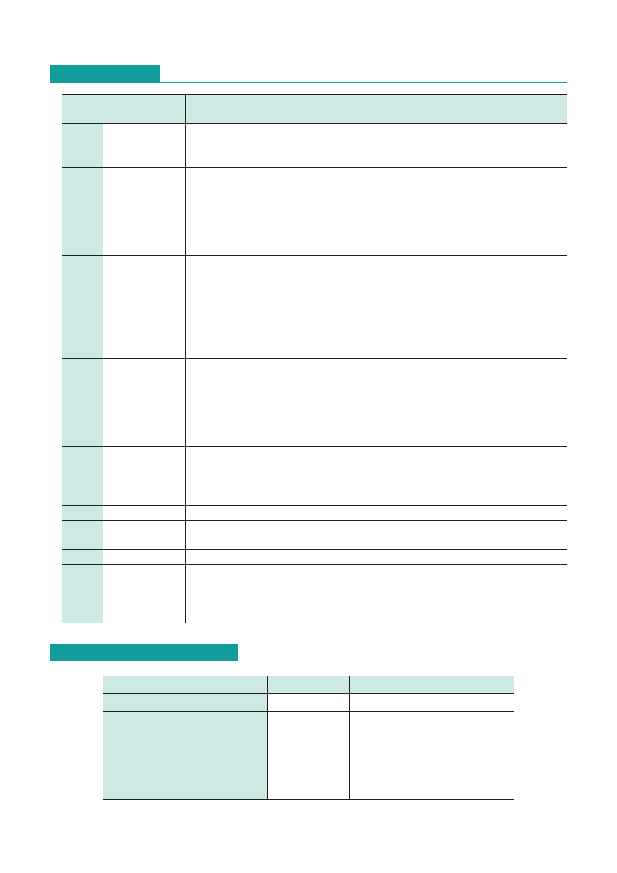
Pin Description
Input/
Pin no. Pin name
output
1
OV Output
2
CS Input
3 DCHG Output
4
PF Output
5
CDC Input
6
COL Input
7
COV Input
8
GND Input
9
V1 Input
10
11
V2 Input
12
13
V3 Input
14
15
V4 Input
16
VCC Input
Function
Overcharge detection output pin
NPN transistor open collector output; normally high impedance, goes to L level on
overdischarge
Overcurrent detection pin
Monitors equivalent load current through source-drain voltage drop of discharge-controlling
FET, and at or above the overcurrent detection voltage sets the DCHG pin to "H" and turns
off the discharge-controlling FET. Following overcurrent detection, current is passed from
this pin, and if the load is decreased, the overcurrent mode is canceled. Through this action
there is a temporary consumption current (at the VCC pin) of approx. 1 mA on resumption of
discharge and detection of overdischarge. This function is disabled in overdischarge mode.
Pin driving the discharge-controlling FET (P-ch)
Normally "L"; on overdischarge set to "H"
Output pin for overdischarge detection signals
Overdischarge detection signal output pin
When the overdischarge detector detects overdischarge at the open collector output
of the NPN transistor, this pin is turned on. A delay is provided by setting a dead
time until discharge ends, so that by utilizing a reset or other signal from a CPU or
some other controlling device, the equipment can be put into standby mode.
Pin to set the dead time for overdischarge detection
By connecting a capacitor between the CDC pin and GND, a dead time can be set.
Pin to set the dead time for overcurrent detection
By connecting a capacitor between the COL pin and GND, a dead time can be set.
If NC, protection is triggered in a short amount of time; the dead time should be
set according to the application.
Pin to set the dead time for overcharge detection
By connecting a capacitor between the COV pin and GND, a dead time can be set.
Ground pin
Pin for input of V1 cell high-side voltage and V2 cell low-side voltage
N.C
Pin for input of V2 cell high-side voltage and V3 cell low-side voltage
N.C
Pin for input of V3 cell high-side voltage and V4 cell low-side voltage
N.C
Pin for input of V4 cell high-side voltage
Power supply input pin
The same potential as the V4 pin should be input
Absolute Maximun Ratings (Ta=25°C)
Item
Storage temperature
Operating temperature
Charge voltage
Power supply voltage
Voltage applied to OV pin
Allowable loss
Symbol
TSTG
TOPR
VV4 max.
VCC max.
VOV max.
Pd
Ratings
-40~+125
-20~+70
24
24
24
300
Units
°C
°C
V
V
V
mW
Share Link: 