M65609E Просмотр технического описания (PDF) - Atmel Corporation
Номер в каталоге
Компоненты Описание
производитель
M65609E Datasheet PDF : 14 Pages
| |||
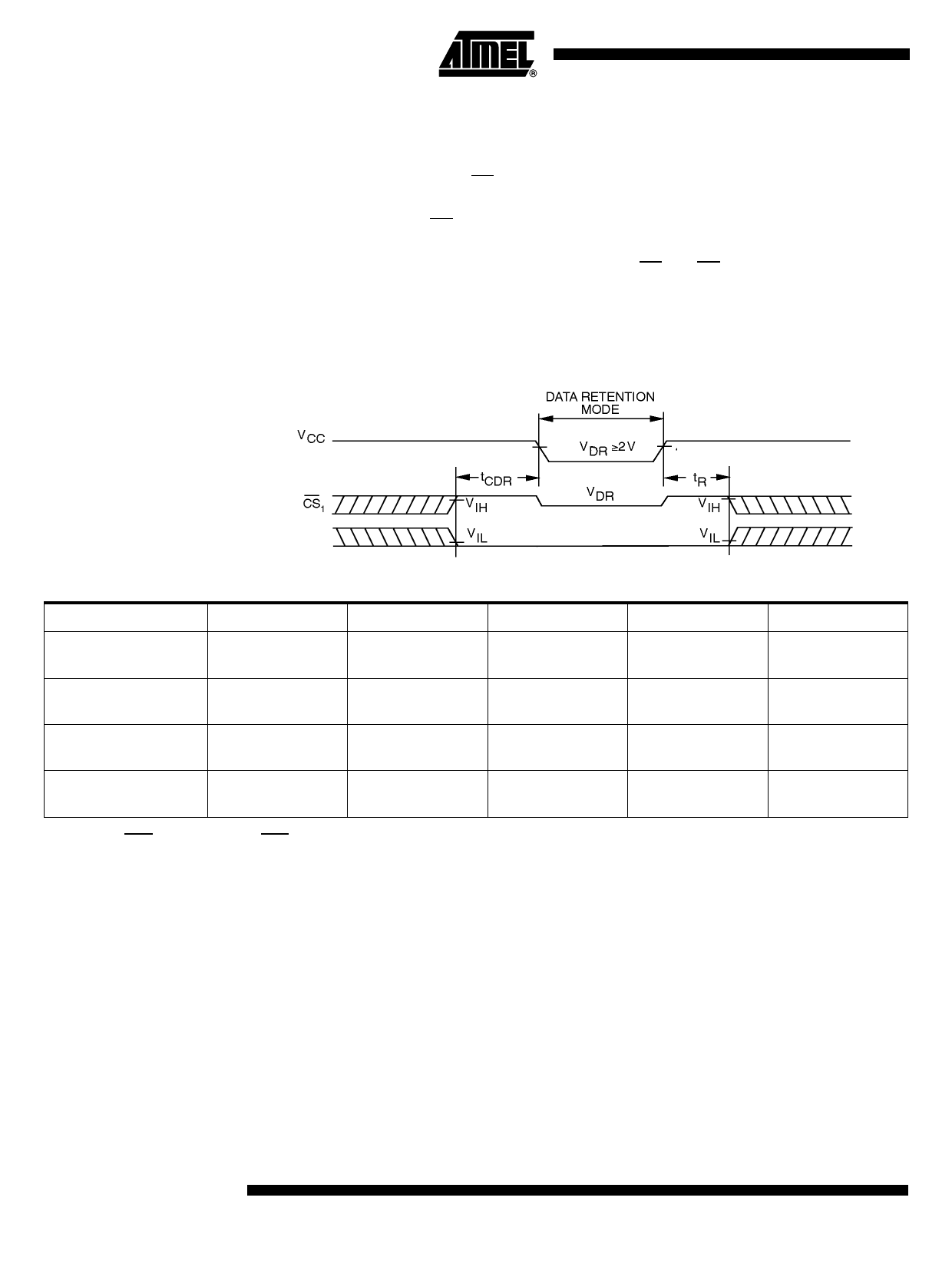
Data Retention Mode
Atmel CMOS RAM’s are designed with battery backup in mind. Data retention voltage
and supply current are guaranteed over temperature. The following rules ensure data
retention:
1. During data retention CS must be held high within VCC to VCC - 0.2V or chip
select BS must be held down within GND to GND +0.2V.
2. Output Enable (OE) should be held high to keep the RAM outputs high imped-
ance, minimizing power dissipation.
3. During power-up and power-down transitions CS and OE must be kept between
VCC + 0.3V and 70% of VCC, or with BS between GND and GND -0.3V.
4. The RAM can begin operation > tR ns after VCC reaches the minimum operation
voltages (3V).
Figure 1. Data Retention Timing
3V
3V
BS
Data Retention Characteristics
Parameter
Description
Min
VCCDR
VCC for data
retention
2.0
TCDR
Chip deselect to
data retention time
0.0
tR
Operation recovery
time
tAVAV(1)
ICCDR1(2)
Data retention
current at 2.0V
–
Notes: 1. TAVAV = Read Cycle Time
2. CS1 = VCC or CS2 = CS1 = GND, VIN = GND/VCC.
Typical TA = 25°C
–
–
–
0.010
Max
–
–
–
1.0
Unit
V
ns
ns
mA
8 M65609E
4158D–AERO–06/02
Share Link: 