M65609E(2007) Просмотр технического описания (PDF) - Atmel Corporation
Номер в каталоге
Компоненты Описание
производитель
M65609E Datasheet PDF : 14 Pages
| |||
M65609E
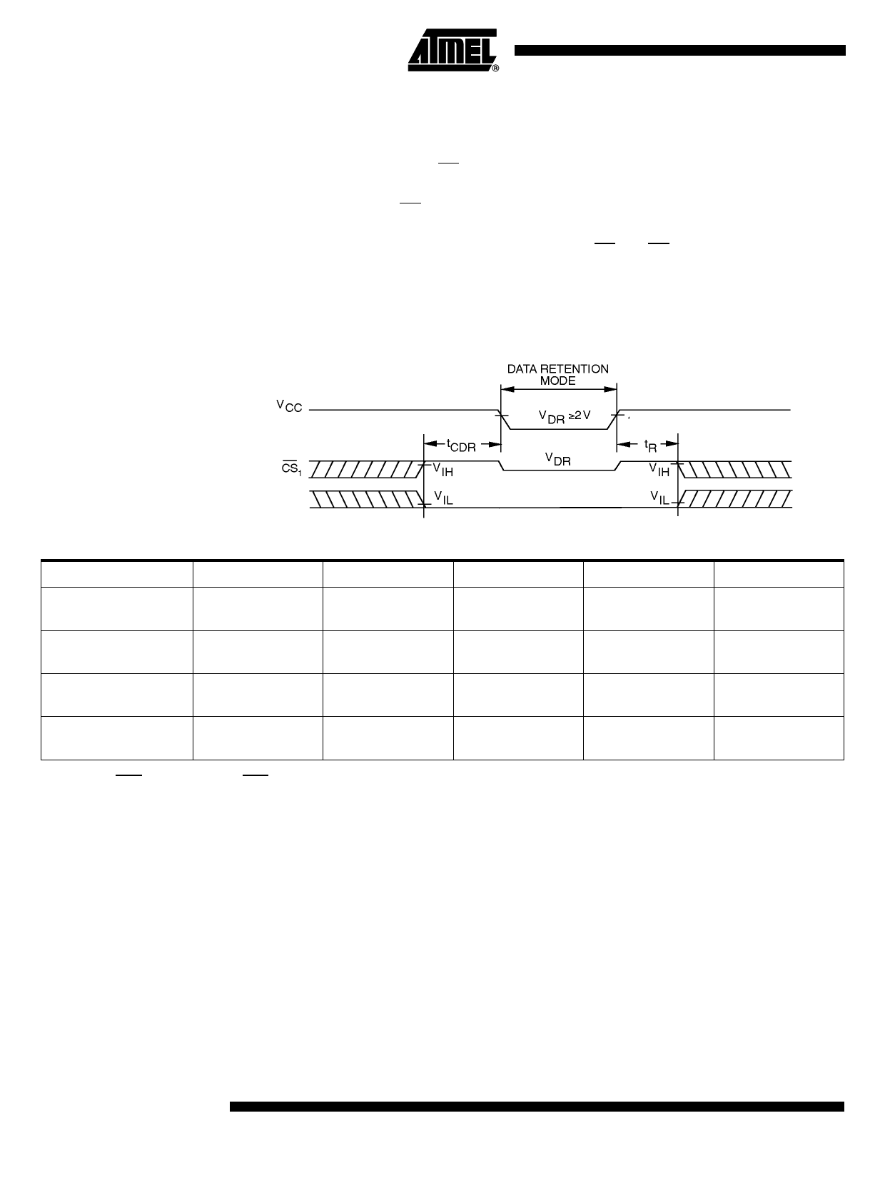
Data Retention Mode
Atmel CMOS RAM’s are designed with battery backup in mind. Data retention voltage
and supply current are guaranteed over temperature. The following rules ensure data
retention:
1. During data retention CS1 must be held high within VCC to VCC - 0.2V or chip
select CS2 must be held down within GND to GND +0.2V.
2. Output Enable (OE) should be held high to keep the RAM outputs high imped-
ance, minimizing power dissipation.
3. During power-up and power-down transitions CS1 and OE must be kept
between VCC + 0.3V and 70% of VCC, or with BS between GND and GND -0.3V.
4. The RAM can begin operation > tR ns after VCC reaches the minimum operation
voltages (3V).
Figure 1. Data Retention Timing
Data Retention Characteristics
Parameter
VCCDR
Description
VCC for data
retention
Min
Typical TA = 25°C
Max
2.0
–
–
TCDR
Chip deselect to
data retention time
0.0
–
–
tR
Operation recovery
time
tAVAV(1)
–
–
ICCDR1(2)
Data retention
current at 2.0V
–
0.010
1.0
Notes: 1. TAVAV = Read Cycle Time
2. CS1 = VCC or CS2 = CS1 = GND, VIN = GND/VCC.
Unit
V
ns
ns
mA
8
4158I–AERO–07/07
Share Link: 