ML7020 Просмотр технического описания (PDF) - Oki Electric Industry
Номер в каталоге
Компоненты Описание
производитель
ML7020 Datasheet PDF : 19 Pages
| |||
1Semiconductor
FEDL7020-02
ML7020
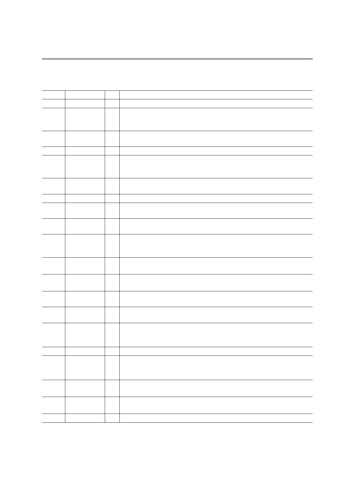
PIN DESCRIPTIONS
Pin No.
1
2
Symbol
VDD
TIO
3
TI–
4
TI+
5
LI1O
6
LI1–
7
LI1+
8
SWI
9
SGO
10
LI2O
11
LI2–
12
TO
13
LO+
14
LO–
15
SGC
16
GND
17
CSB
18
RDB
19
WRB
20
A0
I/O
Description
Power supply pin. Connect a +5 V power supply to this pin.
The output pin of the input amplifier 1. See Figure 1. For the sake of noise
O reduction, connect a capacitor between this pin and TI– (3) so as to attenuate
high frequency components above 10 kHz.
I The inverting input pin for the input amplifier 1. When the input amplifier 1 is not
used, connect pin TIO (2) to pin TI– (3), and connect pin TI+ (4) to pin SGO.
I The non-inverting input pin for the input amplifier 1.
The output pin for the input amplifier 2. See Figure 1. For the sake of noise
O reduction, connect a capacitor between this pin and LI1– (6) so as to attenuate
high frequency components above 10 kHz.
I
The inverting input pin for the input amplifier 2. When the input amplifier 2 is not
used, connect pin LI1O (5) and LI1– (6), and connect pin LI+ (7) to pin SGO.
I The non-inverting input pin for the input amplifier 2.
I The input pin for SW3. This pin is connected internally to SGO (9) when SW3 is
to be made ON.
O The signal ground output pin for external circuits. A voltage of about VDD/2 is
output from this pin.
The output pin for the input amplifier 3. See Figure 1. For the sake of noise
O reduction, connect a capacitor between this pin and LI2– (10) so as to attenuate
high frequency components above 10 kHz.
The inverting input pin for the input amplifier 3.
I
When the input amplifier 3 is not used, connect pin LI2O (10) and LI2– (11).
The output pin of the output amplifier 1.
O
Can drive a load of 1.2 kΩ or more.
O
The non-inverting output pin for the output amplifier 2.
of connecting a peripheral circuit.
See Figure 2 for details
O
The inverting output pin of the output amplifier 2.
connecting a peripheral circuit.
See Figure 2 for details of
The signal ground output pin for internal circuits. A voltage of about VDD/2 is
O output from this pin.
Connect a 1 µF capacitor between SGC (15) and GND (16).
The ground pin for the LSI. Connect a 0 V input to this pin.
The chip select pin for the processor interface.
I Reading and writing are possible when this input is “0”. Reading and writing are
disabled when this input is “1”.
The read control pin for the processor interface.
I
Data can be read from the LSI when this pin is “0”.
The write control pin for the processor interface.
I
Data is written into this LSI at the rising edge of the WR signal.
I The address input pin A0 for the processor interface.
4/19
Share Link: 