ML2021I Просмотр технического описания (PDF) - Fairchild Semiconductor
Номер в каталоге
Компоненты Описание
производитель
ML2021I Datasheet PDF : 11 Pages
| |||
ML2021
PRODUCT SPECIFICATION
Powerdown Mode
A powerdown mode can be selected with pin PDN. When
PDN = 1, the device is powered down. In this state, the power
consumption is reduced by removing power from the analog
section and forcing the analog output, VOUT, to a high
impedance state. While the device is in power down mode,
the digital section is still functional and the current data word
remains stored in the latch. The master clock, CLK, can
be left active or removed during powerdown mode. When
PDN = 0, the device is in normal operation.
Applications
Power Supplies
The digital section inside the device is powered between
VCC and GND, or 5 volts. The analog section is powered
between VCC and VSS, or ±5 volts. The analog section uses
AGND as the reference point.
GND and AGND are totally isolated inside the device to
minimize coupling from the digital section into the analog
section. Typically this is less than 100 µV. However, ANGD
and GND should be tied together physically near the device
and close to the common power supply ground connection.
The power supply rejection of VCC and VSS to the analog
output is greater than –60dB at 1 kHz, typically. If decou-
pling of the power supplies is still necessary in a system,
VCC and VSS should be decoupled with respect to AGND.
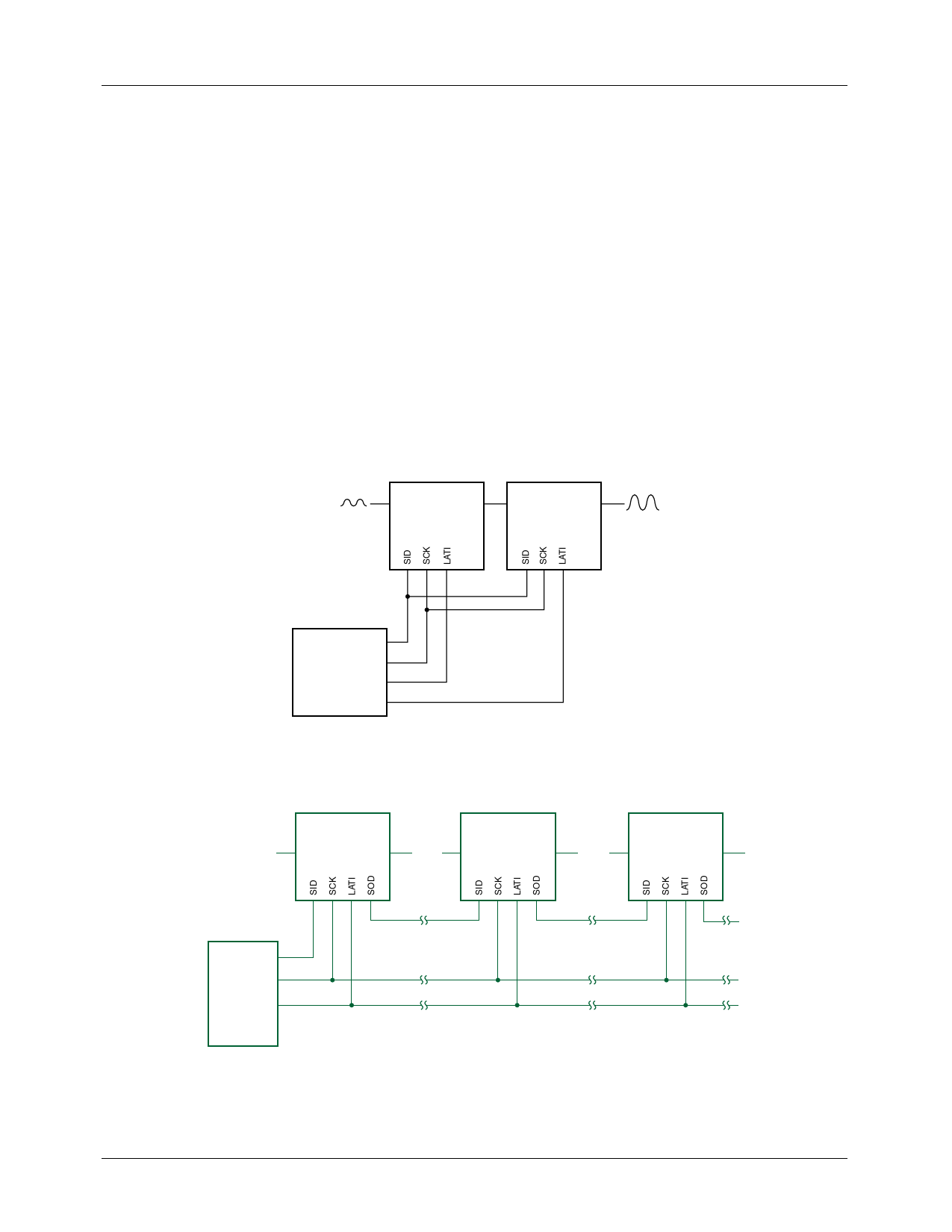
ML2004
LOG GAIN/ATTEN
VIN
VOUT
ML2021
EQUALIZER
VIN
VOUT
µP
Figure 8. Typical Serial Interface
ML2021 OR ML2004
VIN
VOUT
ML2021 OR ML2004
VIN
VOUT
ML2021 OR ML2004
VIN
VOUT
µP
Figure 9. Controlling Multiple ML2021 and ML2004 With
Only 3 Digital Lines Using One Long Data Word
10
REV. 1.1.1 3/19/01
Share Link: 