AD876 Просмотр технического описания (PDF) - Analog Devices
Номер в каталоге
Компоненты Описание
производитель
AD876 Datasheet PDF : 17 Pages
| |||
AD876
analog ground can lower the ac source impedance. The value
of this capacitance will depend on the source resistance and the
required signal bandwidth.
The input span of the AD876 is a function of the reference
voltages. For more information regarding the input range, see
the DRIVING THE REFERENCE TERMINALS section of
the data sheet.
AD876
3
1
AIN
2
CP
CH
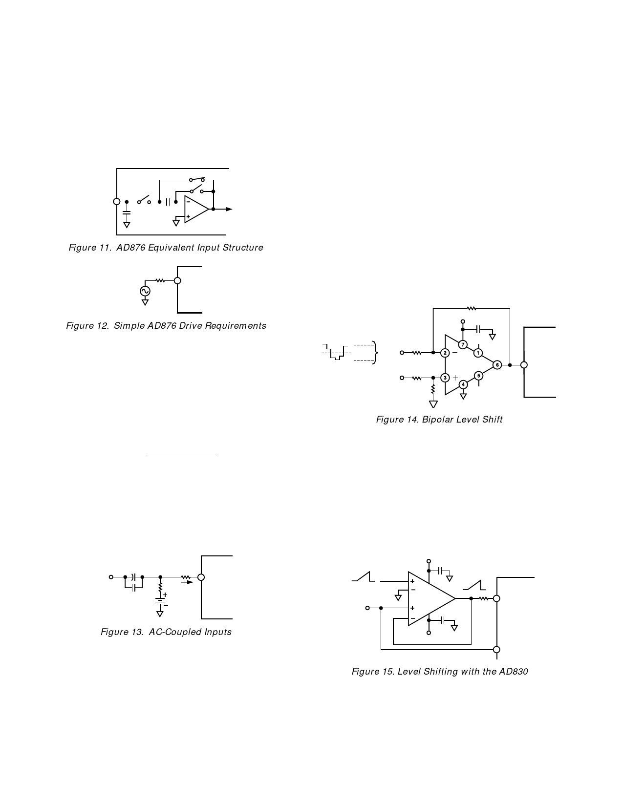
Figure 11. AD876 Equivalent Input Structure
< Ϸ 200⍀
AIN
VS
Figure 12. Simple AD876 Drive Requirements
In many cases, particularly in single-supply operation, ac-
coupling offers a convenient way of biasing the analog input
signal at the proper signal range. Figure 13 shows a typical
configuration for ac-coupling the analog input signal to the
AD876. Maintaining the specifications outlined in the data
sheet requires careful selection of the component values. The
most important concern is the f-3 dB high-pass corner that is a
function of R2, and the parallel combination of C1 and C2.
The f-3 dB point can be approximated by the equation
f
−3 dB
=
[2
×
π
1
× ( R2) Ceq ]
where Ceq is the parallel combination of C1 and C2. Note that
C1 is typically a large electrolytic or tantalum capacitor that
becomes inductive at high frequencies. Adding a small ceramic
or polystyrene capacitor on the order of 0.01 µF that does not
become inductive until negligibly higher frequencies maintains
a low impedance over a wide frequency range.
20 kHz. At a sample clock frequency of 20 MHz, the dc bias
current at 3 V dc is approximately 30 µA. If we choose R2 equal
to 1 kΩ and R1 equal to 50 Ω, the parallel capacitance should
be a minimum of 0.008 µF to avoid attenuating signals close to
20 kHz. Note that the bias current will cause a 31.5 mV offset
from the 3 V bias.
In systems that must use dc-coupling, use an op amp to level-
shift a ground-referenced signal to comply with the input
requirements of the AD876. Figure 14 shows an AD817
configured in inverting mode with ac signal gain of –1. The dc
voltage at the noninverting input of the op amp controls the
amount of dc level shifting. A resistive voltage divider attenu-
ates the REFBF signal. The op amp then multiplies the attenu-
ated signal by 2. In the case where REFBF = 1.6 V, the dc
output level will be 2.6 V. The AD817 is a low cost, fast settling,
single supply op amp with a G = –1 bandwidth of 29 MHz. The
AD818 is similar to the AD817 but has a 50 MHz bandwidth.
Other appropriate op amps include the AD8011, AD812 (a dual),
and the AD8001.
Rf = 4.99k⍀
+VCC
0.1F
0Vdc
2V p-p
RIN = 4.99k⍀
3k⍀
REFBF
14.7k⍀
NC
AD817 OR
AD818
NC
AD876
AIN
Figure 14. Bipolar Level Shift
An integrated difference amplifier such as the AD830 is an
alternate means of providing dc level shifting. The AD830
provides a great deal of flexibility with control over offset and
gain. Figure 15 shows the AD830 precisely level-shifting a
unipolar, ground-referenced signal. The reference voltage,
REFBS, determines the amount of level-shifting. The ac gain
is 1. The AD830 offers the advantages of high CMRR, precise
gain, offset, and high-impedance inputs when compared with a
discrete implementation. For more information regarding the
AD830, see the AD830 data sheet.
C1
VIN
AD876
R1
AIN
C2
3V
R2 IB
VBIAS
2V
0
VB
+12V
0.1
VB +2V
VB
AD830
0.1
AD876
AIN
Figure 13. AC-Coupled Inputs
There are additional considerations when choosing the resistor
values. The ac-coupling capacitors integrate the switching
transients present at the input of the AD876 and cause a net dc
bias current, IB, to flow into the input. The magnitude of this
bias current increases with increasing dc signal level and also
increases with sample frequency. This bias current will result in
an offset error of (R1 + R2) × IB. If it is necessary to compen-
sate this error, consider making R2 negligibly small or modify-
ing VBIAS to account for the resultant offset.
As an example, assume that the input to the AD876 must have
a dc bias of 3 V and the minimum expected signal frequency is
–12V
REFBS
Figure 15. Level Shifting with the AD830
REFERENCE INPUT DRIVING THE REFERENCE
TERMINALS
The AD876 requires an external reference on pins REFTF and
REFBF. The AD876 provides reference sense pins, REFTS
and REFBS, to minimize voltage drops caused by external and
internal wiring resistance. A resistor ladder, nominally 250 Ω,
connects pins REFTF and REFBF.
–8–
REV. B
Share Link: 