AD876 Просмотр технического описания (PDF) - Analog Devices
Номер в каталоге
Компоненты Описание
производитель
AD876 Datasheet PDF : 17 Pages
| |||
AD876
1
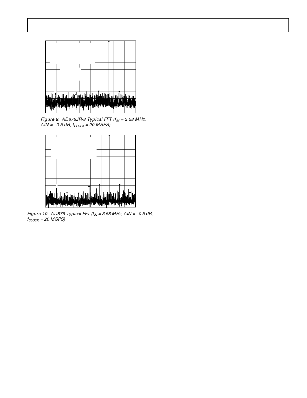
HARMONICS (dBc)
2ND –68.02 6TH –77.74
3RD –72.85 7TH –75.62
4TH –70.68
5TH –78.09
8TH –75.98
9TH –81.20
THD = –64.12
SNR = 48.73
SINAD = 48.61
SFDR = –68.02
2
3
6
98
5
4
7
Figure 9. AD876JR-8 Typical FFT (fIN = 3.58 MHz,
AIN = –0.5 dB, fCLOCK = 20 MSPS)
1
HARMONICS (dBc)
2ND –68.91 6TH –80.55
3RD –73.92 7TH –82.02
4TH –68.67
5TH –73.26
8TH –81.02
9TH –88.94
PIPELINE DELAY (LATENCY)
The number of clock cycles between conversion initiation and
the associated output data being made available. New output
data is provided every clock cycle.
REFERENCE TOP/BOTTOM OFFSET
Resistance between the reference input and comparator input
tap points causes offset errors. These errors can be nulled out
by using the force-sense connection as shown in the Reference
Input section.
THEORY OF OPERATION
The AD876 implements a pipelined multistage architecture to
achieve high sample rate with low power. The AD876 distrib-
utes the conversion over several smaller A/D subblocks, refining
the conversion with progressively higher accuracy as it passes
the results from stage to stage. As a consequence of the distrib-
uted conversion, the AD876 requires a small fraction of the 1023
comparators used in a traditional flash type A/D. A sample-and-
hold function within each of the stages permits the first stage to
operate on a new input sample while the second and third stages
operate on the two preceding samples.
THD = –64.24
SNR = 55.71
SINAD = 55.14
SFDR = –68.67
2
3
5
6
8
9
4
7
Figure 10. AD876 Typical FFT (fIN = 3.58 MHz, AIN = –0.5 dB,
fCLOCK = 20 MSPS)
DEFINITIONS OF SPECIFICATIONS
INTEGRAL NONLINEARITY (INL)
Integral nonlinearity refers to the deviation of each individual
code from a line drawn from “zero” through “full scale”. The
point used as “zero” occurs 1/2 LSB before the first code transi-
tion. “Full scale” is defined as a level 1 1/2 LSB beyond the last
code transition. The deviation is measured from the center of
each particular code to the true straight line.
DIFFERENTIAL NONLINEARITY (DNL, NO MISSING
CODES)
An ideal ADC exhibits code transitions that are exactly 1 LSB
apart. DNL is the deviation from this ideal value. It is often
specified in terms of the resolution for which no missing codes
(NMC) are guaranteed.
OFFSET ERROR
The first transition should occur at a level 1/2 LSB above
“zero.” Offset is defined as the deviation of the actual first code
transition from that point.
GAIN ERROR
The first code transition should occur for an analog value 1/2 LSB
above nominal negative full scale. The last transition should
occur for an analog value 1 1/2 LSB below the nominal positive
full scale. Gain error is the deviation of the actual difference
between first and last code transitions and the ideal difference
between the first and last code transitions.
APPLYING THE AD876
DRIVING THE ANALOG INPUT
Figure 11 shows the equivalent analog input of the AD876, a
sample-and-hold amplifier (SHA). Bringing CLK to a logic low
level closes Switches 1 and 2 and opens Switch 3. The input
source connected to AIN must charge capacitor CH during this
time. When CLK transitions from logic “low” to logic “high,”
Switch 1 opens first, placing the SHA in hold mode. Switch 2
opens subsequently. Switch 3 then closes, connects the feed-
back loop around the op amp, and forces the output of the op
amp to equal the voltage stored on CH. When CLK transitions
from logic “high” to logic “low”, Switch 3 opens first. Switch 2
closes and reconnects the input to CH. Finally, Switch 1 closes
and places the SHA in track mode.
The structure of the input SHA places certain requirements on
the input drive source. The combination of the pin capacitance,
CP, and the hold capacitance, CH, is typically less than 5 pF.
The input source must be able to charge or discharge this ca-
pacitance to 10-bit accuracy in one half of a clock cycle. When
the SHA goes into track mode, the input source must charge or
discharge capacitor CH from the voltage already stored on CH
(the previously captured sample) to the new voltage. In the
worst case, a full-scale voltage step on the input, the input
source must provide the charging current through the RON (50 Ω)
of Switch 2 and quickly settle (within 1/2 CLK period). This
situation corresponds to driving a low input impedance. On the
other hand, when the source voltage equals the value previously
stored on CH, the hold capacitor requires no input current and
the equivalent input impedance is extremely high.
Adding series resistance between the output of the source and
the AIN pin reduces the drive requirements placed on the
source. Figure 12 shows this configuration. The bandwidth of
the particular application limits the size of this resistor. To
maintain the performance outlined in the data sheet specifica-
tions, the resistor should be limited to 200 Ω or less. For appli-
cations with signal bandwidths less than 10 MHz, the user may
increase the size of the series resistor proportionally. Alterna-
tively, adding a shunt capacitance between the AIN pin and
REV. B
–7–
Share Link: 