MJF122(2008) Просмотр технического описания (PDF) - ON Semiconductor
Номер в каталоге
Компоненты Описание
производитель
MJF122 Datasheet PDF : 7 Pages
| |||
MJF122, MJF127
Complementary Power
Darlingtons
For Isolated Package Applications
Designed for general−purpose amplifiers and switching
applications, where the mounting surface of the device is required to
be electrically isolated from the heatsink or chassis.
Features
• Electrically Similar to the Popular TIP122 and TIP127
• 100 VCEO(sus)
• 5.0 A Rated Collector Current
• No Isolating Washers Required
• Reduced System Cost
• High DC Current Gain − 2000 (Min) @ IC = 3 Adc
• UL Recognized, File #E69369, to 3500 VRMS Isolation
• Pb−Free Packages are Available*
MAXIMUM RATINGS
ÎÎÎÎÎÎÎÎÎÎÎÎÎÎÎÎÎÎÎ Rating
Symbol Value
Unit
ÎÎÎÎÎÎÎÎÎÎÎÎÎÎÎÎÎÎÎ Collector−Emitter Voltage
ÎÎÎÎÎÎÎÎÎÎÎÎÎÎÎÎÎÎÎ Collector−Base Voltage
ÎÎÎÎÎÎÎÎÎÎÎÎÎÎÎÎÎÎÎ Emitter−Base Voltage
ÎÎÎÎÎÎÎÎÎÎÎÎÎÎÎÎÎÎÎ RMS Isolation Voltage (Note 1)
(t = 0.3 sec, R.H. ≤ 30%, TA = 25°C)
ÎÎÎÎÎÎÎÎÎÎÎÎÎÎÎÎÎÎÎ Per Figure 14
VCEO
VCB
VEB
VISOL
100
100
5
4500
Vdc
Vdc
Vdc
VRMS
ÎÎÎÎÎÎÎÎÎÎÎÎÎÎÎÎÎÎÎ Collector Current − Continuous
Peak
IC
5
Adc
8
ÎÎÎÎÎÎÎÎÎÎÎÎÎÎÎÎÎÎÎ Base Current
ÎÎÎÎÎÎÎÎÎÎÎÎÎÎÎÎÎÎÎ Total Power Dissipation (Note 2)
ÎÎÎÎÎÎÎÎÎÎÎÎÎÎÎÎÎÎÎ @ TC = 25_C
ÎÎÎÎÎÎÎÎÎÎÎÎÎÎÎÎÎÎÎ Derate above 25_C
IB
0.12
Adc
PD
30
W
0.24
W/_C
Total Power Dissipation @ TA = 25_C
ÎÎÎÎÎÎÎÎÎÎÎÎÎÎÎÎÎÎÎ Derate above 25_C
PD
2
W
0.016 W/_C
ÎÎÎÎÎÎÎÎÎÎÎÎÎÎÎÎÎÎÎ Operating and Storage Junction Temperat- TJ, Tstg −65 to
IC
ÎÎÎÎÎÎÎÎÎÎÎÎÎÎÎÎÎÎÎ ure Range
+ 150
ÎÎÎÎÎÎÎÎÎÎÎÎÎÎÎÎÎÎÎ THERMAL CHARACTERISTICS
ÎÎÎÎÎÎÎÎÎÎÎÎÎÎÎÎÎÎÎ Characteristic
Symbol Max
Unit
Thermal Resistance, Junction−to−Ambient
ÎÎÎÎÎÎÎÎÎÎÎÎÎÎÎÎÎÎÎ Thermal Resistance, Junction−to−Case
ÎÎÎÎÎÎÎÎÎÎÎÎÎÎÎÎÎÎÎ (Note 2)
RqJA
RqJC
62.5
_C/W
4.1
_C/W
ÎÎÎÎÎÎÎÎÎÎÎÎÎÎÎÎÎÎÎ Lead Temperature for Soldering Purpose
TL
260
_C
ÎÎÎÎÎÎÎÎÎÎÎÎÎÎÎÎÎÎÎ Maximum ratings are those values beyond which device damage can occur.
Maximum ratings applied to the device are individual stress limit values (not
normal operating conditions) and are not valid simultaneously. If these limits are
exceeded, device functional operation is not implied, damage may occur and
reliability may be affected.
1. Proper strike and creepage distance must be provided.
2. Measurement made with thermocouple contacting the bottom insulated
mounting surface (in a location beneath the die), the device mounted on a
heatsink with thermal grease and a mounting torque of ≥ 6 in. lbs.
© Semiconductor Components Industries, LLC, 2008
1
September, 2008 − Rev. 7
http://onsemi.com
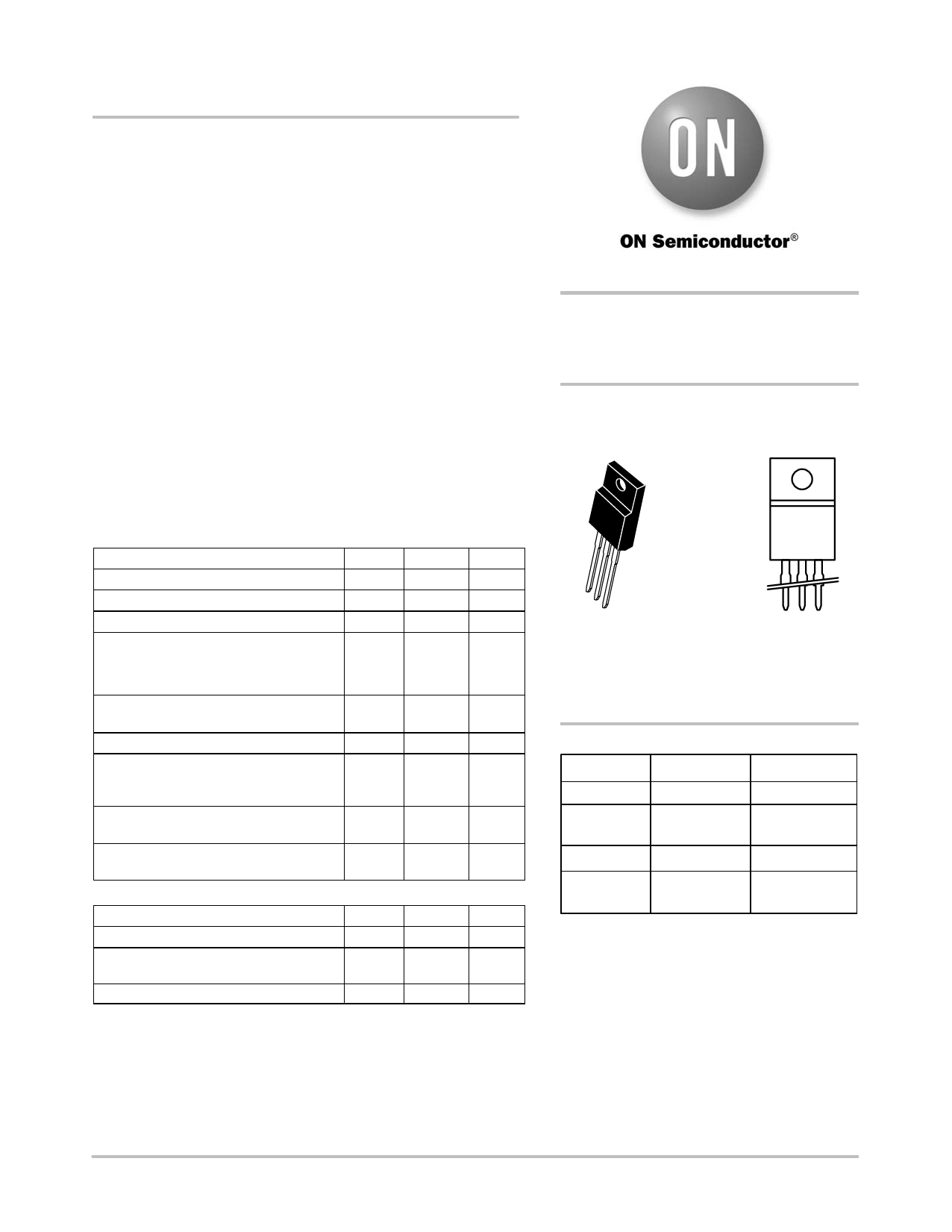
COMPLEMENTARY SILICON
POWER DARLINGTONS
5.0 A, 100 V, 30 W
NPN
COLLECTOR 2
PNP
COLLECTOR 2
BASE
1
BASE
1
EMITTER 3
MJF122
EMITTER 3
MJF127
12
3
MARKING
DIAGRAM
TO−220
CASE 221D−02
STYLE 2
MJF12xG
AYWW
x
= 2 or 7
G
= Pb−Free Package
A
= Assembly Location
Y
= Year
WW
= Work Week
ORDERING INFORMATION
Device
MJF122
Package
TO−220
Shipping†
50 Units / Rail
MJF122G
TO−220
(Pb−Free)
50 Units / Rail
MJF127
TO−220
50 Units / Rail
MJF127G
TO−220
(Pb−Free)
50 Units / Rail
†For information on tape and reel specifications,
including part orientation and tape sizes, please
refer to our Tape and Reel Packaging Specifications
Brochure, BRD8011/D.
*For additional information on our Pb−Free strategy
and soldering details, please download the
ON Semiconductor Soldering and Mounting
Techniques Reference Manual, SOLDERRM/D.
Publication Order Number:
MJF122/D
Share Link: 