2N3055 Просмотр технического описания (PDF) - ON Semiconductor
Номер в каталоге
Компоненты Описание
производитель
2N3055 Datasheet PDF : 4 Pages
| |||
2N3055(NPN), MJ2955(PNP)
ÎÎÎÎÎÎÎÎÎÎÎÎÎÎÎÎÎÎÎÎÎÎÎÎÎÎÎÎÎÎÎÎÎ THERMAL CHARACTERISTICS
ÎÎÎÎÎÎÎÎÎÎÎÎÎÎÎÎÎÎÎÎÎÎÎÎÎÎÎÎÎÎÎÎÎ Characteristic
Thermal Resistance, Junction−to−Case
ÎÎÎÎÎÎÎÎÎÎÎÎÎÎÎÎÎÎÎÎÎÎÎÎÎÎÎÎÎÎÎÎÎÎÎÎÎÎÎÎÎÎÎÎÎÎÎÎÎÎÎÎÎÎÎÎÎÎÎÎÎÎÎÎÎÎ ELECTRICAL CHARACTERISTICS (TC = 25_C unless otherwise noted)
ÎÎÎÎÎÎÎÎÎÎÎÎÎÎÎÎÎÎÎÎÎÎÎÎÎÎÎÎÎÎÎÎÎÎÎÎÎÎÎÎÎÎÎÎÎÎÎÎÎÎÎÎÎÎÎÎÎÎÎÎÎÎÎÎÎÎ Characteristic
Symbol
RqJC
Max
Unit
1.52
_C/W
Symbol
Min
Max
Unit
OFF CHARACTERISTICS*
Collector−Emitter Sustaining Voltage (Note 1) (IC = 200 mAdc, IB = 0)
VCEO(sus)
60
−
Vdc
Collector−Emitter Sustaining Voltage (Note 1) (IC = 200 mAdc, RBE = 100 W)
ÎÎÎÎÎÎÎÎÎÎÎÎÎÎÎÎÎÎÎÎÎÎÎÎÎÎÎÎÎÎÎÎÎ Collector Cutoff Current (VCE = 30 Vdc, IB = 0)
ÎÎÎÎÎÎÎÎÎÎÎÎÎÎÎÎÎÎÎÎÎÎÎÎÎÎÎÎÎÎÎÎÎ Collector Cutoff Current
(VCE = 100 Vdc, VBE(off) = 1.5 Vdc)
ÎÎÎÎÎÎÎÎÎÎÎÎÎÎÎÎÎÎÎÎÎÎÎÎÎÎÎÎÎÎÎÎÎ (VCE = 100 Vdc, VBE(off) = 1.5 Vdc, TC = 150°C)
ÎÎÎÎÎÎÎÎÎÎÎÎÎÎÎÎÎÎÎÎÎÎÎÎÎÎÎÎÎÎÎÎÎ Emitter Cutoff Current (VBE = 7.0 Vdc, IC = 0)
ÎÎÎÎÎÎÎÎÎÎÎÎÎÎÎÎÎÎÎÎÎÎÎÎÎÎÎÎÎÎÎÎÎÎÎÎÎÎÎÎÎÎÎÎÎÎÎÎÎÎÎÎÎÎÎÎÎÎÎÎÎÎÎÎÎÎ ON CHARACTERISTICS* (Note 1)
VCER(sus)
70
−
Vdc
ICEO
ICEX
−
0.7 mAdc
mAdc
−
1.0
−
5.0
IEBO
−
5.0 mAdc
DC Current Gain
hFE
−
(IC = 4.0 Adc, VCE = 4.0 Vdc)
20
70
(IC = 10 Adc, VCE = 4.0 Vdc)
5.0
−
Collector−Emitter Saturation Voltage
(IC = 4.0 Adc, IB = 400 mAdc)
(IC = 10 Adc, IB = 3.3 Adc)
VCE(sat)
Vdc
−
1.1
3.0
Base−Emitter On Voltage (IC = 4.0 Adc, VCE = 4.0 Vdc)
ÎÎÎÎÎÎÎÎÎÎÎÎÎÎÎÎÎÎÎÎÎÎÎÎÎÎÎÎÎÎÎÎÎ SECOND BREAKDOWN
ÎÎÎÎÎÎÎÎÎÎÎÎÎÎÎÎÎÎÎÎÎÎÎÎÎÎÎÎÎÎÎÎÎ Second Breakdown Collector Current with Base Forward Biased
ÎÎÎÎÎÎÎÎÎÎÎÎÎÎÎÎÎÎÎÎÎÎÎÎÎÎÎÎÎÎÎÎÎ (VCE = 40 Vdc, t = 1.0 s, Nonrepetitive)
ÎÎÎÎÎÎÎÎÎÎÎÎÎÎÎÎÎÎÎÎÎÎÎÎÎÎÎÎÎÎÎÎÎ DYNAMIC CHARACTERISTICS
ÎÎÎÎÎÎÎÎÎÎÎÎÎÎÎÎÎÎÎÎÎÎÎÎÎÎÎÎÎÎÎÎÎ Current Gain − Bandwidth Product (IC = 0.5 Adc, VCE = 10 Vdc, f = 1.0 MHz)
ÎÎÎÎÎÎÎÎÎÎÎÎÎÎÎÎÎÎÎÎÎÎÎÎÎÎÎÎÎÎÎÎÎ *Small−Signal Current Gain (IC = 1.0 Adc, VCE = 4.0 Vdc, f = 1.0 kHz)
ÎÎÎÎÎÎÎÎÎÎÎÎÎÎÎÎÎÎÎÎÎÎÎÎÎÎÎÎÎÎÎÎÎÎÎÎÎÎÎÎÎÎÎÎÎÎÎÎÎÎÎÎÎÎÎÎÎÎÎÎÎÎÎÎÎÎ *Small−Signal Current Gain Cutoff Frequency (VCE = 4.0 Vdc, IC = 1.0 Adc, f = 1.0 kHz)
VBE(on)
Is/b
fT
hfe
fhfe
−
1.5
Vdc
2.87
−
Adc
2.5
−
MHz
15
120
−
10
−
kHz
*Indicates Within JEDEC Registration. (2N3055)
1. Pulse Test: Pulse Width v 300 ms, Duty Cycle v 2.0%.
20
50 ms
10
dc
1 ms
6
4
500 ms
2
250 ms
1
0.6
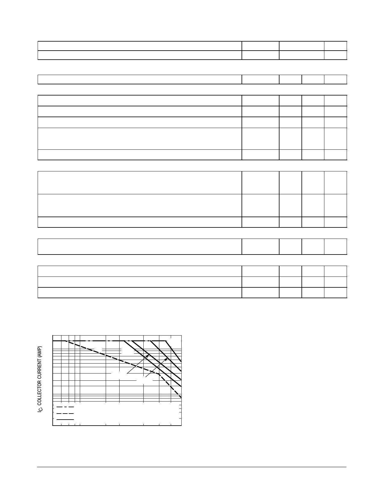
BONDING WIRE LIMIT
0.4
THERMALLY LIMITED @ TC = 25°C (SINGLE PULSE)
SECOND BREAKDOWN LIMIT
0.2
6
10
20
40
60
VCE, COLLECTOR−EMITTER VOLTAGE (VOLTS)
Figure 2. Active Region Safe Operating Area
There are two limitations on the power handling ability of
a transistor: average junction temperature and second
breakdown. Safe operating area curves indicate IC − VCE
limits of the transistor that must be observed for reliable
operation; i.e., the transistor must not be subjected to greater
dissipation than the curves indicate.
The data of Figure 2 is based on TC = 25°C; TJ(pk) is
variable depending on power level. Second breakdown
pulse limits are valid for duty cycles to 10% but must be
derated for temperature according to Figure 1.
http://onsemi.com
2
Share Link: 