MICRF007 –ü—Ä–æ—Å–º–æ—Ç—Ä —Ç–µ—Ö–Ω–∏—á–µ—Å–∫–æ–≥–æ –æ–ø–∏—Å–∞–Ω–∏—è (PDF) - Micrel
–ù–æ–º–µ—Ä –≤ –∫–∞—Ç–∞–ª–æ–≥–µ
–ö–æ–º–ø–æ–Ω–µ–Ω—Ç—ã –û–ø–∏—Å–∞–Ω–∏–µ
–ø—Ä–æ–∏–∑–≤–æ–¥–∏—Ç–µ–ª—å
MICRF007 Datasheet PDF : 13 Pages
| |||
MICRF007
∆V = droop voltage
For example, if user desires ∆t = 10ms and chooses a 4.7µF
CAGC, then the allowable droop is about 144mV. Using the
same equation with 200nA, the worst case pin leakage, and
assuming 1µA of capacitor leakage in the same direction,
the maximum allowable ∆t (shutdown time) is about 0.56s
for droop recovery in 10ms.
The ratio of decay-to-attack time-constant is fixed at 1:10
(that is, the attack time constant is 10 times of the delay time
constant). Generally, the design value of 1:10 is adequate for
the vast majority of applications. If adjustment is required,
adding a resistor in parallel of the CAGC capacitor may vary
the ratio. The value of the resistor must be determined on a
case by case basis.
Additional Applications Information
In addition to the basic operation of the MICRF007, the fol-
lowing enhancements can be made. In particular, it is strongly
recommended that the antenna impedance is matched to
the input of the IC.
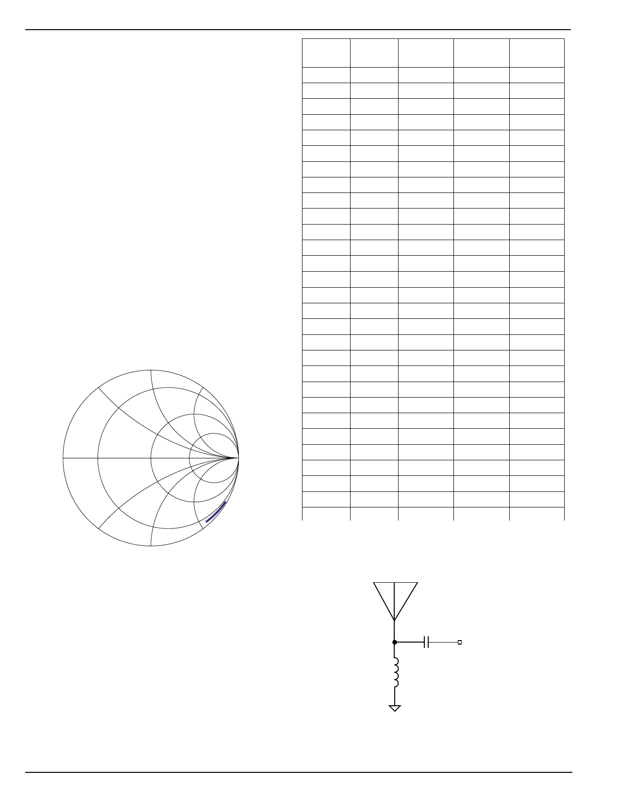
Antenna Impedance Matching
As shown in Figure 2 and Table 3, the antenna pin input
impedance is frequency dependent.
The ANT pin can be matched to 50Ω with a high pass circuit
as shown in Figure 3. That is, a shunt inductor from the
antenna input to ground and a capacitor in series from the
antenna input to the ANT pin.
j25
j100
0
50
ÔøΩ
–j25
–j100
Micrel
Frequency
(MHz)
ZIN(Ω)
Z11
S11
CSERIES (pF)
LSHUNT (nH)
300
12– j166 0.803– j0.529
1.5
62
305
12– j165 0.800– j0.530
1.4
62
310
12 – j163 0.796– j0.536
1.6
56
315
13 – j162 0.791– j0.536
1.5
56
320
12 – j160 0.789– j0.543
1.4
56
325
12 – j157 0.782– j0.550
1.7
51
330
12 - j155 0.778– j0.556
1.5
51
335
12 – j152 0.770– j0.564
1.4
51
340
11 - j150 0.767– j0.572
1.6
47
345
11 – j148 0.762– j0.578
1.5
47
350
11 – j145 0.753– j0.586
1.4
47
355
11 – j143 0.748– j0.592
1.6
43
360
11 – j141 0.742– j0.597
1.5
43
365
11 – j139 0.735– j0.603
1.4
43
370
10 – j137 0.732– j0.61
1.3
43
375
10 – j135 0.725– j0.619
1.6
39
380
10 – j133 0.718– j0.625
1.4
39
385
10 – j131 0.711– j0.631
1.3
39
390
10 – j130 0.707– j0.634
1.2
39
395
10 – j128 0.700– j0.641
1.5
36
400
10 – j126 0.692– j0.647
1.4
36
405
10 – j124 0.684– j0.653
1.2
36
410
10 – j122 0.675– j0.660
1.5
33
415
10 – j120 0.667– j0.667
1.4
33
420
10 – j118 0.658– j0.673
1.3
33
425
10 – j117 0.653– j0.677
1.6
30
430
10 – j115 0.643– j0.684
1.5
30
435
10 – j114 0.638– j0.687
1.4
30
440
8 – j112 0.635– j0.704
1.2
30
Table 4. Input Impedance vs. Frequency
Figure 2. Impedance Looking into Antenna Pin
M9999-021705
CSERIES
LSHUNT
ANT Pin
Figure 3. Antenna Impedance Matching Network
8
February 17, 2005
Share Link: 