MIC5031 Просмотр технического описания (PDF) - Micrel
Номер в каталоге
Компоненты Описание
производитель
MIC5031 Datasheet PDF : 8 Pages
| |||
MIC5031
Functional Description
Refer to “Functional Diagram.”
The MIC5031 is a noninverting device. Applying a CMOS
logic high signal to EN (enable input) activates the driver’s
internal circuitry. Applying a TTL logic high signal to CTL
(control input) produces gate drive output. The G (gate)
output is used to turn on an external N-channel MOSFET.
Control
CTL (control) is a TTL compatible input. The threshold is
approximately 1.4V, independent of the supply voltage.
The falling edge of a signal applied to CTL also resets the
overcurrent lockout latch.
Enable
EN (enable) is a CMOS compatible input. EN enables or
disables all internal circuitry. The enable threshold is approxi-
mately half the supply voltage. The MIC5031 supply current
is near zero when the driver is disabled (low). See “Applica-
tions Information: Power-Up Sequence.”
Charge Pump
The charge pump produces a voltage that is higher than the
supply voltage. This higher voltage is required to drive the
external N-channel MOSFET in high-side switch circuits.
The charge pump consists of an oscillator and a voltage
tripler. When the driver is enabled, the charge pump is
switched on and off to regulate its output voltage.
External capacitors C1 and C2 are required. The charge
pump will not operate without these capacitors.
Bootstrap Capacitor
The external bootstrap capacitor is necessary to achieve the
fastest gate rise times. The bootstrap capacitor (C3) supplies
additional current at a higher voltage to the gate drive
regulator as the MOSFET is switched on.
When the MOSFET is off, the gate drive regulator voltage is
applied to the boost capacitor . As the MOSFET turns on, the
MOSFET source-to-ground voltage increases. The increas-
ing source voltage is added to the voltage across the capaci-
tor for a voltage doubling effect.
Gate Drive Regulator
The gate drive regulator manages the voltage from the
bootstrap capacitor, the supply, and the charge pump.
The gate drive regulator charges the bootstrap capacitor
when the MOSFET is off and limits the voltage from the
bootstrap capacitor as the MOSFET is switched on. It also
performs skip-mode control by switching the charge pump on
and off to regulate the gate drive output voltage.
Gate Output
When the MIC5031 is enabled and CTL is high, the gate
driver steers regulated voltage to G (gate output). When CTL
is low, the gate driver grounds G. This respectively charges
or discharges the external MOSFET’s gate, .
Micrel
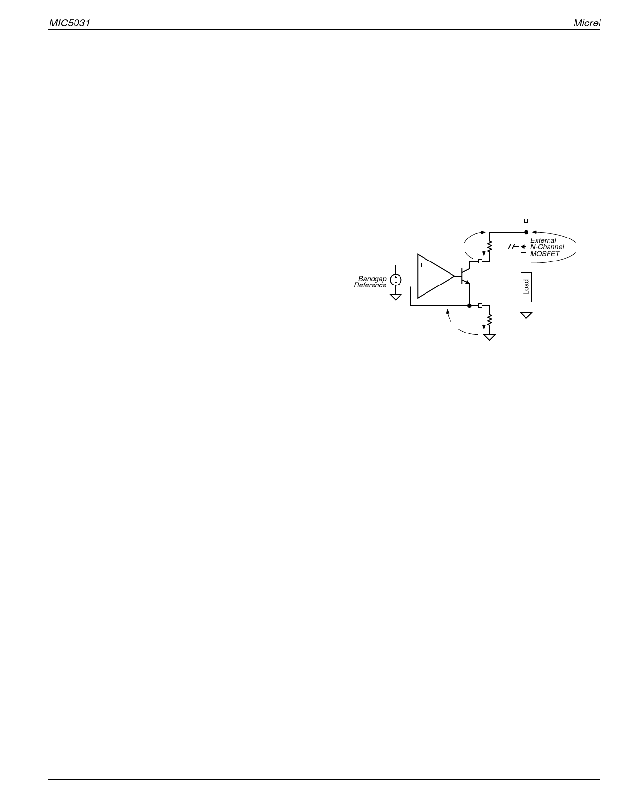
Current Sense
Refer to the “Voltage Reference (Simplified)” diagram.
The MIC5031 detects an overcurrent condition by comparing
the voltage drop across the external MOSFET to a reference
voltage drop created across R1. If VDS exceeds VR1, a
comparator (not shown) shuts off the external MOSFET by
way of the current limit delay, lockout latch, and logic.
The bandgap reference, op amp and NPN create a constant
voltage (1.23V) across R2. This results in a constant current,
IR2, through R2. Ignoring a small amount of base current, the
same current (IR2) flows through R1. R1 is selected to
achieve the desired reference voltage drop, VR1. Refer to the
applications section for formulas.
Supply
1.23V
Bandgap
Reference
VR1 IR2 R1
RV
RI
IR2 R2
1.23V
External
N-Channel VDS
MOSFET
Voltage Reference (Simplified)
An overcurrent condition also activates the fault flag output
when the lockout latch is activated.
Overcurrent-Shutdown Delay
The overcurrent-shutdown delay circuit permits a delay be-
tween overcurrent detection and latch activation for high-
inrush current loads.
The delay can be increased by adding capacitance from DLY
to GND.
Open-Load Detect
The open load detect resistor is an external high-value pull-
up resistor that causes the source voltage of the external
MOSFET to increase when the load is missing.
The MIC5031 monitors the S-pin voltage only when the gate
driver is off. If the voltage on the S-pin rises above the open-
load detect threshold, the fault flag is activated.
Overtemperature Detect
The overtemperature detect circuit switches the logic to turn
the output off at approximately 140°C. An overtemperature
shutdown condition is restored to normal automatically When
the device cools to about 130°C (10°C hysteresis).
An overtemperature condition also activates the fault flag
output.
Fault Flag
FLT (fault flag) is an open-collector NPN transistor. Fault is
active (pulls collector near ground) upon overcurrent, open-
load, or overtemperature.
August 1999
5
MIC5031
Share Link: 