MIC3202 Просмотр технического описания (PDF) - Micrel
Номер в каталоге
Компоненты Описание
производитель
MIC3202 Datasheet PDF : 19 Pages
| |||
Micrel, Inc.
MIC3202/MIC3202-1
Ordering Information (1)
Part Number
Marking
Junction Temperature Range
MIC3202YME
MIC3202YME
−40°C to +125°C
MIC3202-1YME
MIC3202-1YME
−40°C to +125°C
Note:
1. YM® is a GREEN RoHS-compliant package. Lead finish is NiPdAu. Mold compound is Halogen Free.
Package
8-Pin SOIC
8-Pin SOIC
PWM
Dither
Non-Dither
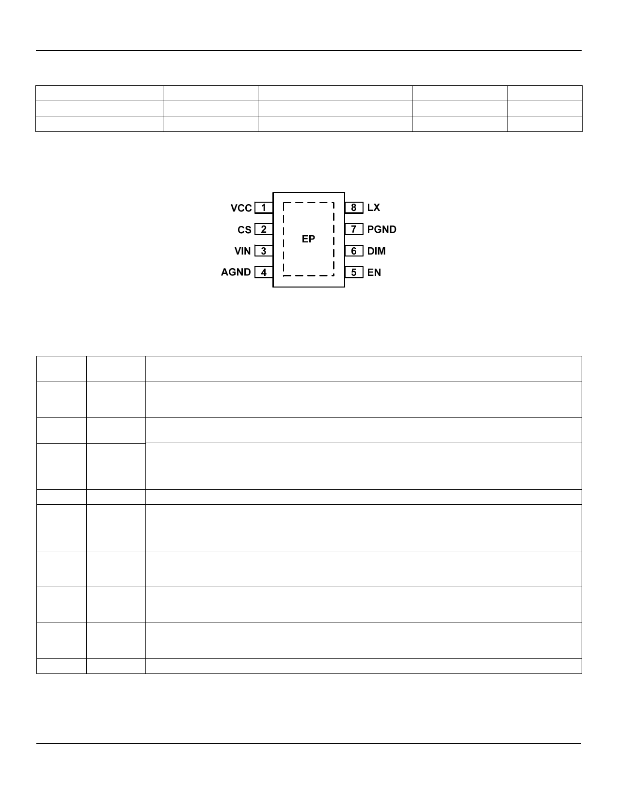
Pin Configuration
8-Pin ePAD SOIC
MIC3202/MIC3202-1
Pin Description
Pin
Number
1
2
3
4
5
6
7
8
EP
Pin Name Pin Function
VCC
CS
VIN
AGND
EN
DIM
PGND
LX
GND
Voltage Regulator Output. The VCC pin supplies the power to the internal circuitry. The VCC is the output
of a linear regulator which is powered from VIN. A 1µF ceramic capacitor is recommended for bypassing
and should be placed as close as possible to the VCC and AGND pins.
Current-Sense Input. The CS pin provides the high-side current sense to set the LED current using an
external sense resistor.
Input Power Supply. The VIN pin is the input supply pin to the internal circuitry and the positive input to
the current sense comparator. Due to the high frequency switching noise, a 1µF ceramic capacitor is
recommended to be placed as close as possible to VIN pin and the power ground (PGND) pin for
bypassing. Please refer to layout recommendations.
Ground pin for analog circuitry. Internal signal ground for all low power sections.
Enable Input. The EN pin provides a logic level control of the output. The voltage has to be 2.0V or higher
to enable the current regulator. The output stage is also gated by the DIM input. When the EN pin is
pulled low, the regulator goes to off state and the supply current of the device is greatly reduced (below
1µA).
PWM Dimming Input. The DIM pin provides the control for brightness of the LED. A PWM input can be
used to control the brightness of LED. DIM high enables the output and its voltage has to be at least 2.0V
or higher. DIM low disables the output, regardless of EN “high” state.
Power Ground pin for Internal Power FET. Power Ground (PGND) is the ground path for the high current.
The current loop for the power ground should be as small as possible and separate from the Analog
ground (AGND) loop. Refer to the layout considerations for more details.
Drain of Internal Power MOSFET. The LX pin connects directly to the inductor and provides the switching
current necessary to operate in hysteretic mode. Due to the high frequency switching and high voltage
associated with this pin, the switch node should be routed away from sensitive nodes.
Connect to PGND.
September 2010
2
M9999-091710-A
Share Link: 