MIC2169 Просмотр технического описания (PDF) - Micrel
Номер в каталоге
Компоненты Описание
производитель
MIC2169 Datasheet PDF : 15 Pages
| |||
MIC2169
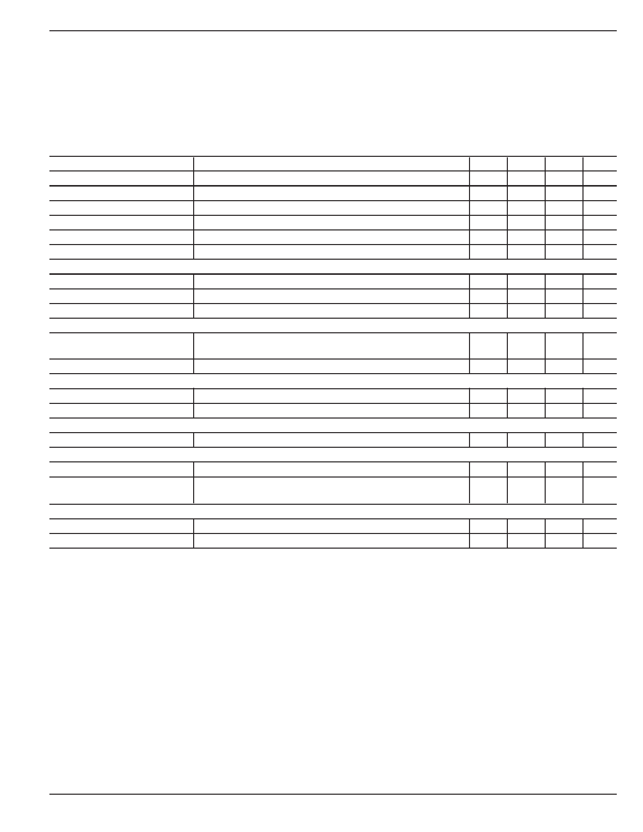
Absolute Maximum Ratings(1)
Supply Voltage (VIN)................................................... 15.5V
Booststrapped Voltage (VBST) .................................VIN +5V
Junction Temperature (TJ) ..................–40°C ≤ TJ ≤ +125°C
Storage Temperature (TS) ........................ –65°C to +150°C
Micrel
Operating Ratings(2)
Supply Voltage (VIN)..................................... +3V to +14.5V
Output Voltage Range .......................... 0.8V to VIN × DMAX
Package Thermal Resistance
θJA 10-lead MSOP ............................................. 180°C/W
Electrical Characteristics(3)
TJ = 25°C, VIN = 5V; bold values indicate –40°C < TJ < +125°C; unless otherwise specified.
Parameter
Condition
Min Typ Max Units
Feedback Voltage Reference
(± 1%)
0.792 0.8 0.808 V
Feedback Voltage Reference
(± 2% over temp)
0.784 0.8 0.816 V
Feedback Bias Current
30
100
nA
Output Voltage Line Regulation
0.03
%/V
Output Voltage Load Regulation
Output Voltage Total Regulation
Oscillator Section
3V ≤ VIN ≤ 14.5V; 1A ≤ IOUT ≤ 10A; (VOUT = 2.5V)(4)
0.5
%
0.6
%
Oscillator Frequency
450 500 550 kHz
Maximum Duty Cycle
Minimum On-Time(4)
92
%
30
60
ns
Input and VDD Supply
PWM Mode Supply Current
VCS = VIN –0.25V; VFB = 0.7V (output switching but excluding
external MOSFET gate current.)
1.5
3
mA
Digital Supply Voltage (VDD)
Error Amplifier
VIN ≥ 6V
4.7
5
5.3
V
DC Gain
70
dB
Transconductance
1
ms
Soft-Start
Soft-Start Current
After timeout of internal timer. See “Soft-Start” section.
8.5
μA
Current Sense
CS Over Current Trip Point
Temperature Coefficient
ppm/°C
VCS = VIN –0.25V
160 200 240
μA
+1800
Output Fault Correction Thresholds
Upper Threshold, VFB_OVT
Lower Threshold, VFB_UVT
(relative to VFB)
(relative to VFB)
+3
%
–3
%
Notes:
1. Absolute maximum ratings indicate limits beyond which damage to the component may occur. Electrical specifications do not apply when operating
the device outside of its operating ratings. The maximum allowable power dissipation is a function of the maximum junction temperature, TJ(max),
the junction-to-ambient thermal resistance, θJA, and the ambient temperature, TA. The maximum allowable power dissipation will result in excessive
die temperature, and the regulator will go into thermal shutdown.
2. Devices are ESD sensitive, handling precautions required.
3. Specification for packaged product only.
4. Guaranteed by design.
March 2009
3
M9999-032409
Share Link: 