MCT7818BT Просмотр технического описания (PDF) - Motorola => Freescale
Номер в каталоге
Компоненты Описание
производитель
MCT7818BT Datasheet PDF : 12 Pages
| |||
MCT7800
APPLICATIONS INFORMATION
Design Considerations
The MCT7800 Series of fixed voltage regulators are
designed with thermal overload protection that shuts down
the circuit when subjected to an excessive power overload
condition, internal short circuit protection that limits the
maximum current the circuit will pass, and output transistor
safe-area compensation that reduces the output short circuit
current as the voltage across the pass transistor is increased.
In many low current applications, compensation capacitors
are not required. However, it is recommended that the
regulator input be bypassed with a capacitor if the regulator is
connected to the power supply filter with long wire lengths, or
if the output load capacitance is large. An input bypass
capacitor should be selected to provide good high frequency
characteristics to insure stable operation under all load
conditions. A 0.33 µF or larger tantalum, mylar, or other
capacitor having low internal impedance at high frequencies,
should be chosen. The bypass capacitor should be mounted
with the shortest possible leads directly across the regulators’
input terminals. Normally, good construction techniques
should be used to minimize ground loops and lead resistance
drops since the regulator has no external sense lead.
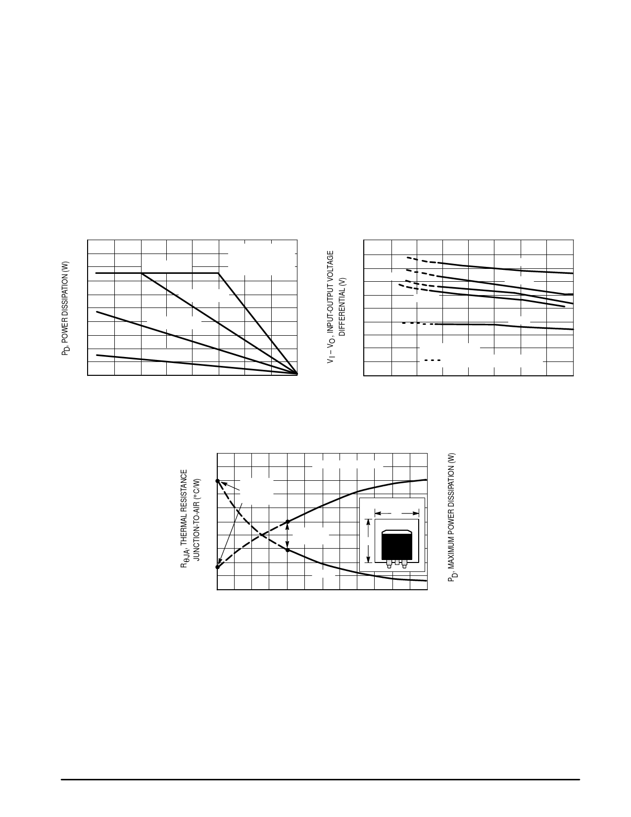
Figure 6. Worst Case Power Dissipation versus
Ambient Temperature (Case 221A)
20
θJC = 5°C/W
16
θHS = 0°C/W
θJA = 65°C/W
TJ(max) = +150°C
12
θHS = 5°C/W
8.0
θHS = 15°C/W
Figure 7. Input Output Differential as a
Function of Junction Temperature
2.5
2.0
200 mA
1.5
20 mA
IO = 1.0 A
500 mA
1.0
0 mA
4.0
No Heatsink
0
– 50 – 25
0 25 50
75 100 125 150
TA, AMBIENT TEMPERATURE (°C)
0.5
∆VO = 2% of VO
– – – Extended Curve for MCT78XXB
0
–75 – 50 – 25 0 25 50 75
TJ, JUNCTION TEMPERATURE (°C)
100 125
Figure 8. D2PAK Thermal Resistance and Maximum
Power Dissipation versus P.C.B. Copper Length
80
3.5
70
60
50
40
Free Air
Mounted
Vertically
PD(max) for TA = 50°C
3.0
ÎÎÎÎÎÎÎÎÎÎÎÎ Minimum
ÎÎÎÎÎÎÎÎÎÎÎÎ Size Pad
2.0 oz. Copper 2.5
L
2.0
L
1.5
RθJA
30
1.0
0
5.0
10
15
20
25
30
L, LENGTH OF COPPER (mm)
DEFINITIONS
Line Regulation — The change in output voltage for a
change in the input voltage. The measurement is made under
conditions of low dissipation or by using pulse techniques
such that the average chip temperature is not significantly
affected.
Load Regulation — The change in output voltage for a
change in load current at constant chip temperature.
Maximum Power Dissipation — The maximum total
device dissipation for which the regulator will operate within
specifications.
MOTOROLA
Quiescent Current — That part of the input current that is
not delivered to the load.
Output Noise Voltage — The rms AC voltage at the
output, with constant load and no input ripple, measured over
a specified frequency range.
Long Term Stability — Output voltage stability under
accelerated life test conditions with the maximum rated
voltage listed in the devices’ electrical characteristics and
maximum power dissipation.
MCT7800
9
Share Link: 