MCP73828-4.1VUATR Просмотр технического описания (PDF) - Microchip Technology
Номер в каталоге
Компоненты Описание
производитель
MCP73828-4.1VUATR
Microchip Technology

MCP73828-4.1VUATR Datasheet PDF : 24 Pages
| |||
MCP73828
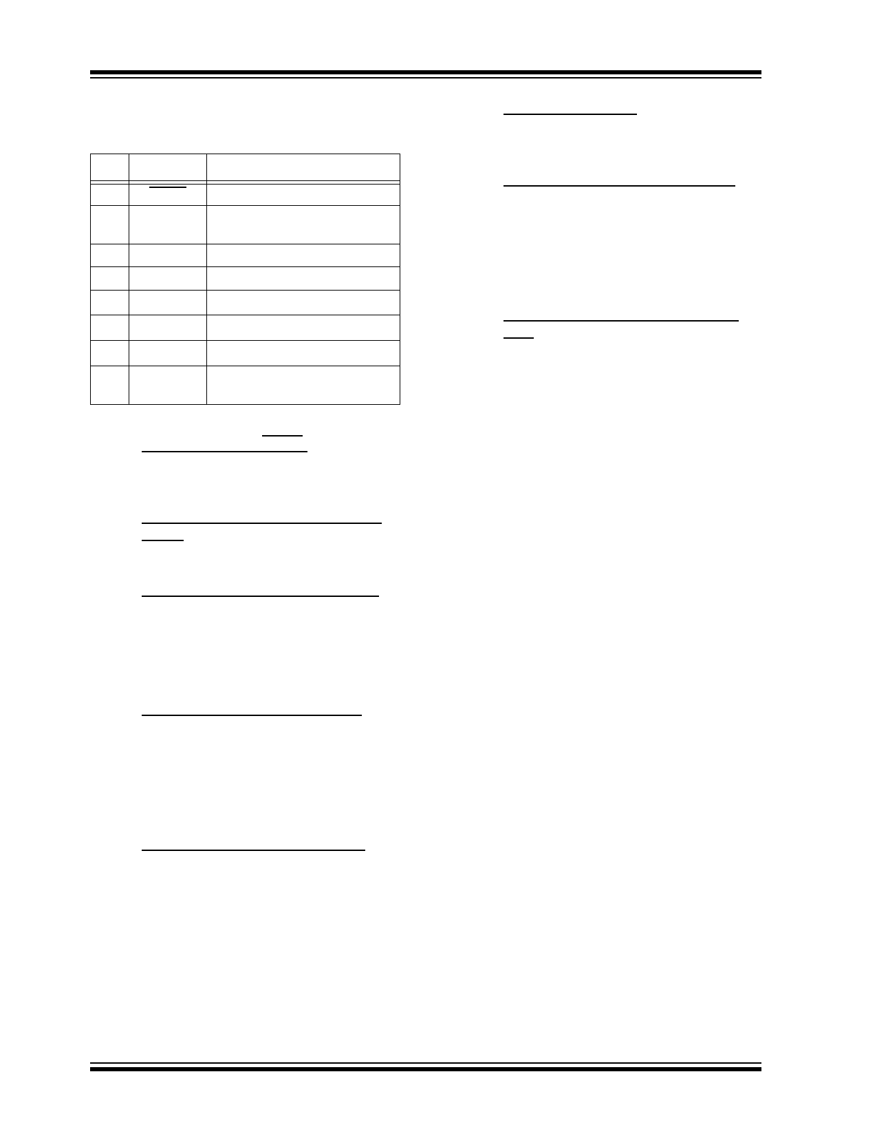
3.0 PIN DESCRIPTION
The descriptions of the pins are listed in Table 3-1.
Pin Name
Description
1
SHDN Logic Shutdown
2
GND Battery Management
0V Reference
3 THERM Cell Temperature Monitor
4
CD10 Charge Complete Output
5
VBAT Cell Voltage Monitor Input
6
VDRV Drive Output
7
VSNS Charge Current Sense Input
8
VIN
Battery Management
Input Supply
TABLE 3-1: Pin Function Table.
3.1 Logic Shutdown (SHDN)
Input to force charge termination, initiate charge, or ini-
tiate recharge.
3.2 Battery Management 0V Reference
(GND)
Connect to negative terminal of battery.
3.3 Cell Temperature Monitor (THERM)
Charging is inhibited when the input is outside the
upper and lower threshold limits. Connection of a
10 kΩ resistor between THERM and GND disables the
function when cell temperature monitoring is not
required.
3.4 Charge Complete Output (CD10)
Open-drain drive for connection to an LED for charge
complete indication. Alternatively, a pull-up resistor can
be applied for interfacing to a microcontroller. A low
impedance state indicates charging. A high impedance
indicates that the charge current has diminished below
10% of the peak charge current.
3.5 Cell Voltage Monitor Input (VBAT)
Voltage sense input. Connect to positive terminal of
battery. Bypass to GND with a minimum of 10 µF to
ensure loop stability when the battery is disconnected.
A precision internal resistor divider regulates the final
voltage on this pin to VREG.
3.6 Drive Output (VDRV)
Direct output drive of an external P-channel MOSFET
pass transistor for current and voltage regulation.
3.7 Charge Current Sense Input VSNS)
Charge current is sensed via the voltage developed
across an external precision sense resistor. The sense
resistor must be placed between the supply voltage
(VIN) and the source of the external pass transistor. A
50 mΩ sense resistor produces a fast charge current of
1 A, typically.
3.8 Battery Management Input Supply
(VIN)
A supply voltage of 4.5V to 5.5V is recommended.
Bypass to GND with a minimum of 10 µF.
DS21706A-page 8
2002 Microchip Technology Inc.
Share Link: