MCP1612T-ADJI/MF(2005) Просмотр технического описания (PDF) - Microchip Technology
Номер в каталоге
Компоненты Описание
производитель
MCP1612T-ADJI/MF Datasheet PDF : 22 Pages
| |||
MCP1612
3.0 MCP1612 PIN DESCRIPTIONS
The descriptions of the pins are listed in Table 3-1.
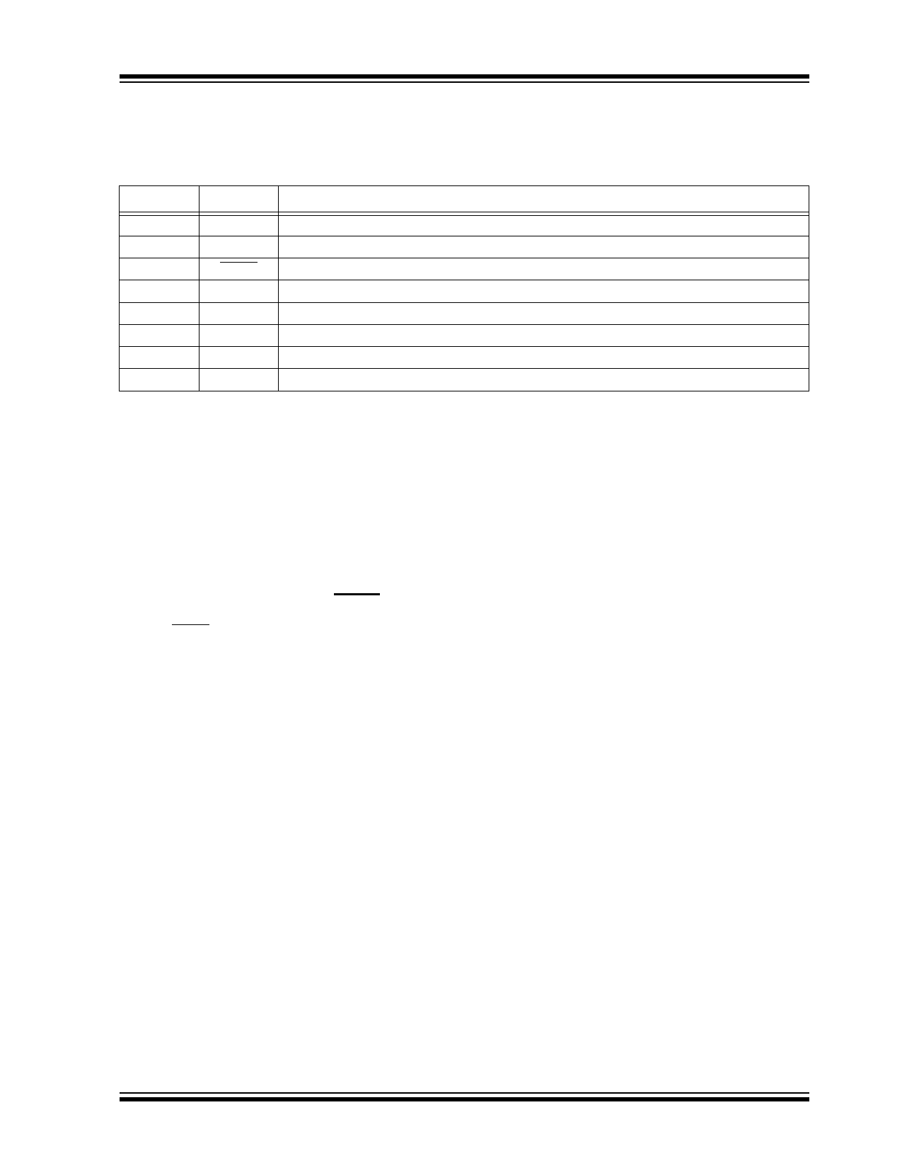
TABLE 3-1:
Pin No.
1
2
3
4
5
6
7
8
PIN FUNCTION TABLE
Name
Function
VIN
VCC
SHDN
COMP
FB
AGND
PGND
LX
Input Voltage Pin
Analog Input Voltage Pin
Shutdown Control Input Pin
Transconductance Amplifier Output Pin
Feedback Input Pin
Analog Ground Pin
Power Ground Pin
Buck Inductor Output Pin
3.1 Input Voltage Pin (VIN)
Connect the input voltage source to VIN. For normal
operation, the voltage on VIN should be between +2.7V
and +5.5V. A 10 µF bypass capacitor should be
connected between VIN and PGND.
3.2 Analog Input Voltage Pin (VCC)
VCC provides bias for internal analog functions. This
voltage is derived by filtering the VIN supply.
3.3 Shutdown Input Pin (SHDN)
Connect SHDN to a logic-level input in order to turn the
regulator on or off. A logic-high (>45% of VIN) will
enable the regulator. A logic-low (<15% of VIN) will
force the regulator into Shutdown mode. When in
shutdown, both the P-channel and N-channel switches
are turned off.
3.4 Compensation Pin (COMP)
COMP is the internal transconductance amplifier
output pin. External compensation is connected to
COMP for control-loop stabilization.
3.5 Feedback Pin (FB)
Connect the output voltage of the buck converter
through an external resistor divider to FB to regulate
the output voltage. The nominal voltage compared to
this input for pulse termination is 0.8V.
3.6 Analog Ground Pin (AGND)
Tie all small-signal ground returns to AGND. Noise on
AGND can effect the sensitive internal analog
measurements.
3.7 Power Ground Pin (PGND)
Connect all large-signal ground returns to PGND. These
large-signal traces should have a small loop area and
length to prevent coupling of switching noise to
sensitive traces.
3.8 Buck Inductor Output Pin (LX)
Connect LX directly to the buck inductor. This pin
carries large signal-level currents; all connections
should be made as short as possible.
© 2005 Microchip Technology Inc.
DS21921B-page 9
Share Link: 