MCM36F9 Просмотр технического описания (PDF) - Motorola => Freescale
Номер в каталоге
Компоненты Описание
производитель
MCM36F9 Datasheet PDF : 11 Pages
| |||
AC OPERATING CONDITIONS AND CHARACTERISTICS
(VDD = 3.3 V + 10%, – 5%, TA = 0 to 70°C, Unless Otherwise Noted)
Input Timing Measurement Reference Level . . . . . . . . . . . . . . 1.25 V
Input Pulse Levels . . . . . . . . . . . . . . . . . . . . . . . . . . . . . . . . . 0 to 2.5 V
Input Rise/Fall Time . . . . . . . . . . . . . . . . . . . . . . . 1 V/ns (20 to 80%)
Output Timing Reference Level . . . . . . . . . . . . . . . . . . . . . . . . . 1.25 V
Output Load . . . . . . . . . . . . . . See Figure 1 Unless Otherwise Noted
DATA RAM READ/WRITE CYCLE TIMING (See Notes 1, 2, 3, and 4)
MCM36F8 – 10
MCM36F9 – 10
Parameter
Symbol
Min
Max
Unit
Cycle Time
Clock Access Time
Output Enable to Output Valid
Clock High to Output Active
Clock High to Output Change
Output Enable to Output Active
Output Disable to Q High–Z
Clock High to Q High–Z
Clock High Pulse Width
Clock Low Pulse Width
Setup Times:
tKHKH
15
tKHQV
—
tGLQV
—
tKHQX1
0
tKHQX2
2
tGLQX
0
tGHQZ
—
tKHQZ
2
tKHKL
4.5
tKLKH
4.5
Address
tAVKH
2
ADSP
tADKH
Data In
tDVKH
Write
tWVKH
Chip Enable
tEVKH
—
ns
10
ns
3.5
ns
—
ns
—
ns
—
ns
3.5
ns
3.5
ns
—
ns
—
ns
—
ns
Hold Times:
Address
tKHAX
0.5
ADSP, ADSC, ADV
tKHADX
Data In
tKHDX
Write
tKHWX
Chip Enable
tKHEX
—
ns
NOTES:
1. Write is defined as either any BWx and SW low or WE is low.
2. Chip Enable is defined as E0 low, SE2 high, and SE3 low whenever ADSP or ADSC is asserted.
3. All read and write cycle timings are referenced from K0 or G0.
4. G0 is a don’t care after write cycle begins. To prevent bus contention, G0 should be negated prior to start of write cycle.
5. This parameter is sampled and not 100% tested.
6. Measured at ± 200 mV from steady state.
Notes
5
5
5
5, 6
5, 6
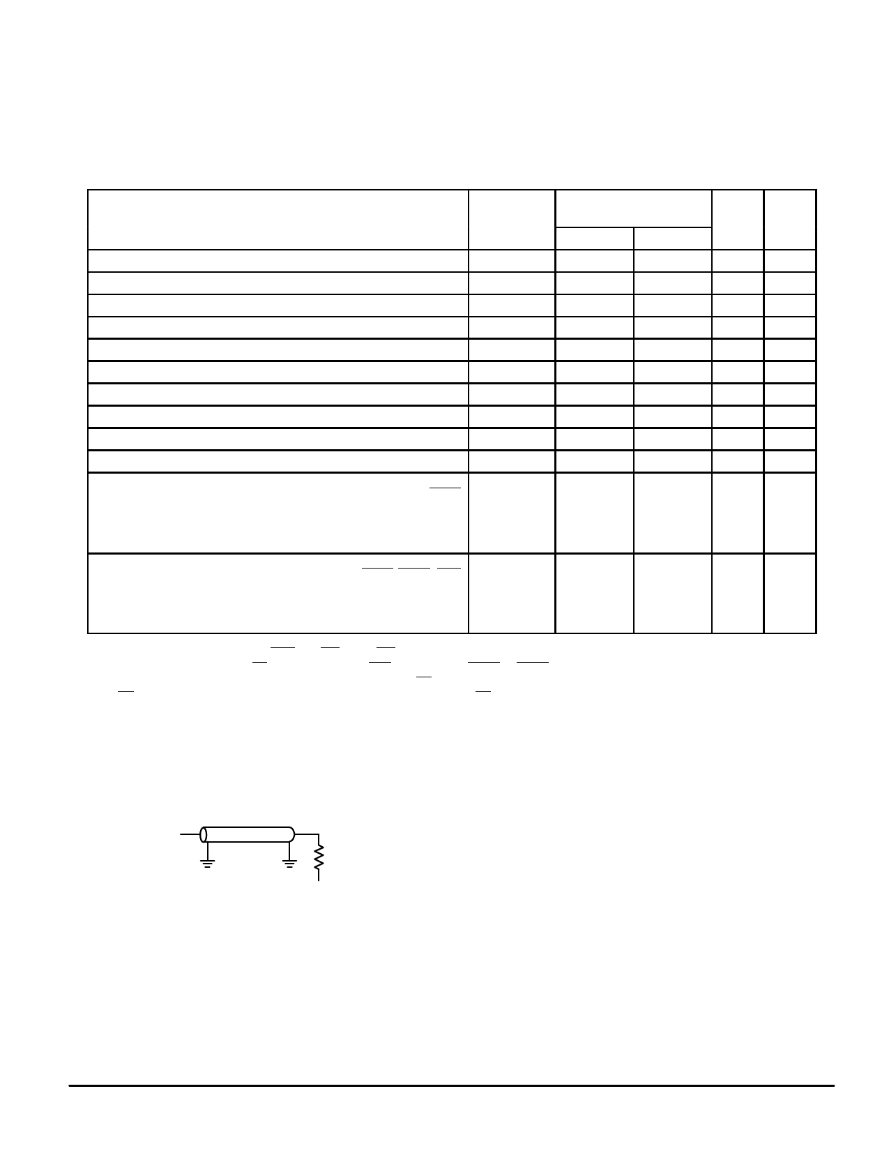
OUTPUT
Z0 = 50 Ω
50 Ω
VL = 1.25 V
TIMING LIMITS
The table of timing values shows either a minimum or a
maximum limit for each parameter. Input requirements are
specified from the external system point of view. Thus, ad-
dress setup time is shown as a minimum since the system
must supply at least that much time (even though most
devices do not require it). On the other hand, responses
from the memory are specified from the device point of
view. Thus, the access time is shown as a maximum since
the device never provides data later than that time.
Figure 1. AC Test Load
MCM36F8•MCM36F9
8
MOTOROLA FAST SRAM
Share Link: 