MC44605(2000) Просмотр технического описания (PDF) - ON Semiconductor
Номер в каталоге
Компоненты Описание
производитель
MC44605
(Rev.:2000)
(Rev.:2000)
ON Semiconductor

MC44605 Datasheet PDF : 20 Pages
| |||
MC44605
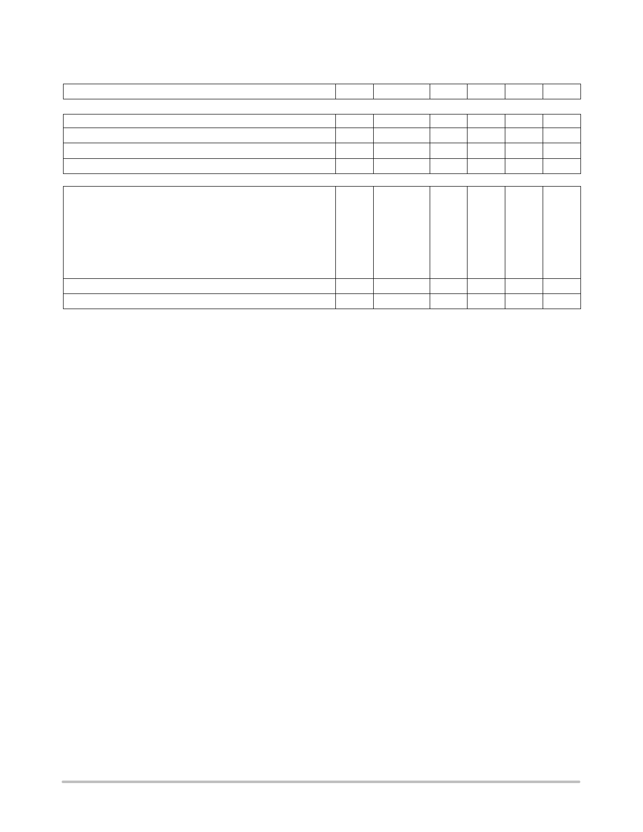
ELECTRICAL CHARACTERISTICS (VCC and VC = 12 V, Rref = 10 kΩ, CT = 2.2 nF, for typical values TA = 25°C, for min/max
values TA = –25° to +85°C unless otherwise noted.) (Note 1.)
Characteristic
Pin #
Symbol
Min
Typ
Max
Unit
OVERVOLTAGE SECTION
Propagation Delay (VCC > 18.1 V to Vout Low)
TPHL(In/Out) 1.0
–
4.0
µs
Protection Level on VCC (TA = –25° to +85°C)
EHT OVP SECTION (Note 2.)
VCC prot
15.9
–
18.1
V
Negative Clamp Level (Isynch–in = –2.0 mA)
NEG–SYNC –0.65
–0.5
–0.35
V
EHT OVP Input Threshold
EHT OVP Input Bias Current (VEHT OVP(pin 9) = 0 V)
Vref
7.0
7.4
7.8
V
9
IEHTOVP
–5.0
–
0
µA
WINDING SHORT CIRCUIT DETECTION SECTION
WSCD Threshold with Ipin15 = 200 µA
Vshift
70
100
120
mV
MPL & OHD SECTION
MPL Parameter*
ΓMPL
0.185
0.240
0.295
V–1
MPL Comparator Threshold**
OHD Parameter***
VMPL–th
2.4
2.5
2.6
V
ΓOHD
1.15
1.50
1.85
V–1
OHD Comparator Threshold****
VOHD–th
2.4
2.5
2.6
V
*This parameter is defined in the MPL §. This parameter is obtained by measuring the MPL pin average current and dividing this result by the
corresponding squared VCS, the measured frequency value and the CT value deducted from the measured frequency value.
" Measurement conditions: VFeedback(pin 14) = 2.3 V, Vsoft–start(pin 11) = 0.5 V and pins 7, 8, and 9 connected to GND (the working frequency
is typically equal to 18 kHz – Rref = 10 kΩ 1%, CT = 2.2 nF).
**The MPL comparator output is DisMPL.
***This parameter is defined in the OHD §. This parameter is obtained by measuring the OHD pin average current and dividing this result by
the corresponding squared VCS value and multiplying it by the Rref value.
" Measurement conditions: VFeedback(pin 14) = 2.3 V, Vsoft–start(pin 11) = 0.5 V and pins 7, 8, and 9 connected to GND (the working frequency
is typically equal to 18 kHz – Rref = 10 kΩ 1%, CT = 2.2 nF).
****The OHD comparator output is DisOHD.
DISABLING BLOCK SECTION
Delay Pulse Width
Ratio (EHTOVP and WSCD Disabling Capacitor Charge
Current)Iref
TWSCD
–
4.0
–
µs
IDis–H/Iref
90
100
110
%
Ratio (MPL and OHD Disabling Capacitor Charge Current)Iref
IDis–L/Iref
2.7
3.1
3.5
%
Minimum VCC Value Enabling the Disabling Block Latch*
VCCDis
1.0
–
5.0
V
*Once a fault detection activated it, the Disabling Block Latch gets reset when the VCC becomes lower than this threshold.
TOTAL DEVICE
Power Supply Current
Startup–Up (VCC = 5.0 V with VCC increasing)
Startup–Up (VCC = 9.0 V with VCC increasing)
Startup–Up (VCC = 12 V with VCC increasing)
Operating TA = –25°C to +85°C*
Disabling Mode (VCC = 6.0 V)**
Power Supply Zener Voltage (ICC = 35 mA)
Thermal Shutdown
ICC
mA
–
0.35
0.55
–
0.35
0.55
–
0.35
0.55
–
20
25
–
–
0.55
VZ
18.5
–
–
V
–
–
155
–
°C
*Refer to Note 1.
**This consumption is measured while the circuit is inhibited by the Definitive Latch.
1. Adjust VCC above the start–up threshold before setting to 12 V. Low duty cycle pulse techniques are used during test to maintain junction
temperature as close to ambient as possible.
2. This function can be inhibited by connecting pin 9 to GND. In this case, the synchronization block is inhibited too and the MC44605 works
in free mode.
http://onsemi.com
6
Share Link: