MC33566 Просмотр технического описания (PDF) - ON Semiconductor
Номер в каталоге
Компоненты Описание
производитель
MC33566 Datasheet PDF : 8 Pages
| |||
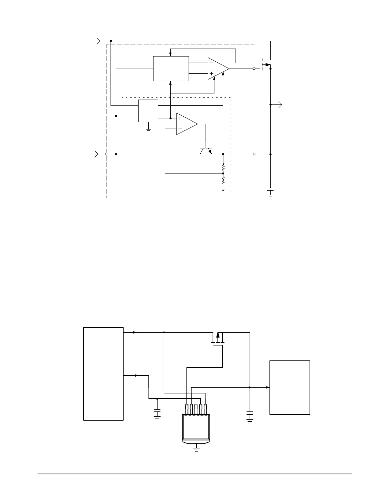
+3.3 Vaux
MC33566
Compensation
&
Hysteresis
Hyst sw
Comp
Driver Drive out
Ref &
Detect Vref
5V detect
External
P-channel
MOSFET
+3.3 Vout
+5 Vin
+3.3 Vout
LDO
Figure 2. Functional Block Diagram
External
4.7 µF
cap
FUNCTIONAL DESCRIPTION
Input Blocking – The internal NPN pass transistor of the
LDO regulator ensures that no significant reverse current
will flow from +3.3 Vout back to the +5.0 Vin input when the
5.0 V input is not powered and the 3.3 Vin supply is present.
5.0 Volt Detect – Internal circuitry detects the presence of
the 5.0 V input supply. When the 5.0 V supply drops below
a given threshold, the +3.3 Vin bypass transistor (an external
P–channel MOSFET) is enabled. The 5.0 V detect logic is
active throughout the entire range of ramp–up from 0 to
5.5 V. Additionally, the drive out signal is never turned ON
or OFF inappropriately during ramp–up of the +5.0 Vin
supply. Also, +3.3 Vout never drops below 3.0 V while
+5.0 Vin is above the 5.0 V detect minimum threshold.
Glitch–free Transfer – The design of the 5.0 V detect
circuitry and drive out control circuitry guarantees that the
+3.3 Vout will not exceed the output voltage specification
listed in the table of DC Operating Specifications even with
+5.0 Vin ramping up and down at the extremes of the slew
rates in the table of AC Operating Specifications.
Offset Voltage Performance – To ensure performance
when external offsets are present on the +5.0 Vin and
+3.3 Vin power inputs, the device has been designed to be
capable of operating with either one or both of these inputs
rising from or falling to zero volts, or with offsets of 0.05 V
to 0.9 V as the inputs ramp up and down.
3.3V aux
Motherboard/
Mainboard
5V
PCI Slot
4.7 µF
5432 1
D VGV V
R ON I A
DNU
X
PCI Card
Circuitry
4.7 µF
Figure 3. Application Block Diagram
http://onsemi.com
4
Share Link: 