MC33566 Просмотр технического описания (PDF) - ON Semiconductor
Номер в каталоге
Компоненты Описание
производитель
MC33566 Datasheet PDF : 8 Pages
| |||
MC33566
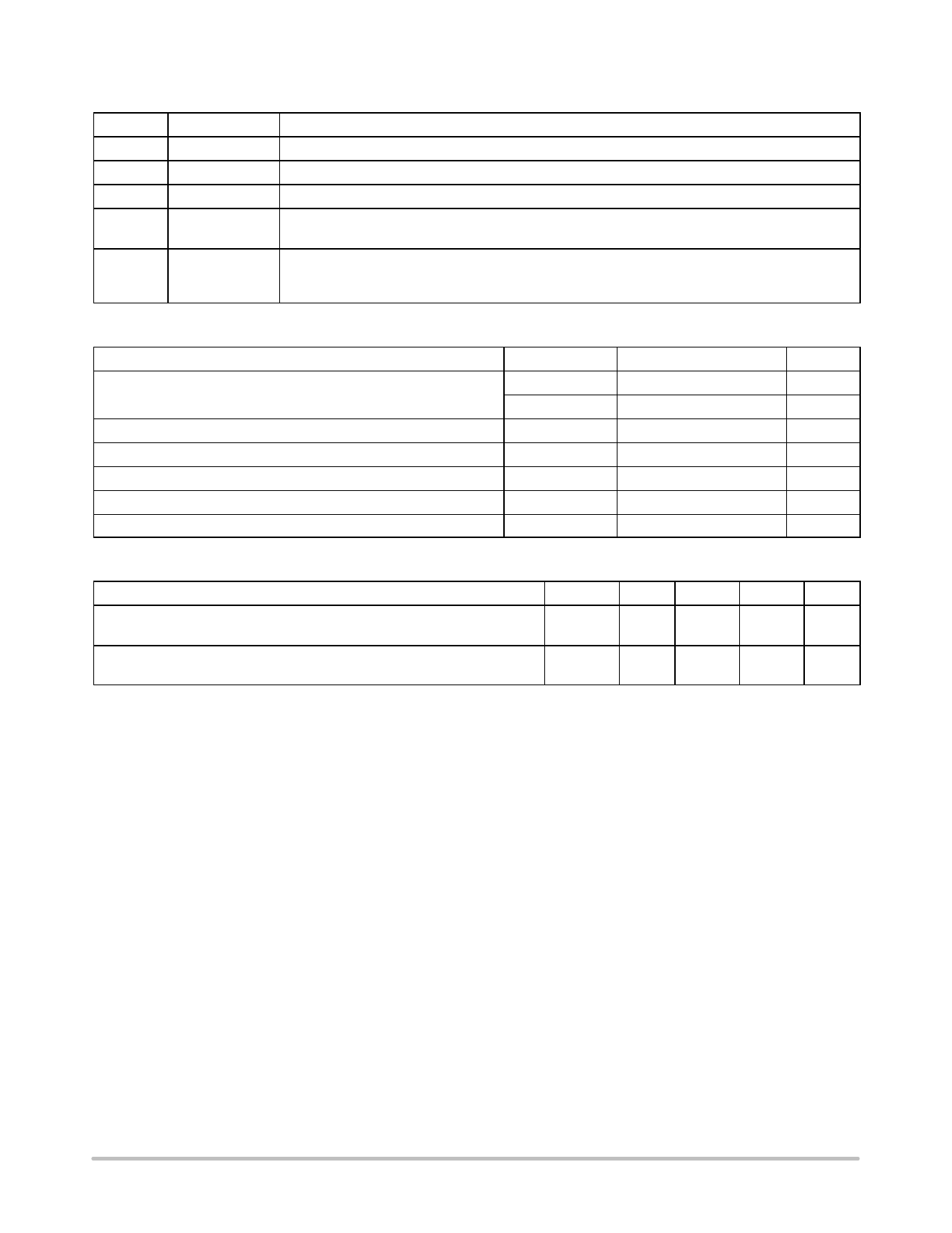
PIN ASSIGNMENTS AND FUNCTIONS
Pin #
Pin Name
Pin Description
1
+3.3 Vaux
Auxiliary input. Typical voltage 3.3 V.
2
+5.0 Vin
This is the input supply for the IC. Typical voltage 5.0 V. (Notes 1. and 2.)
3
Gnd
Logic and power ground.
3.3 V output provided to the application circuit (output current is sourced to this pin from the
4
+3.3 Vout
5.0 V input.)
This output drives a P–channel MOSFET with up to 2000 pF of “effective” gate capacitance.
5
Drive out
Recommended devices are the MMFT5P03HD and MTSF1P02HD. Drive out has active internal
pull–up and pull–down circuitry to guarantee fast transitions.
MAXIMUM RATINGS (TC = 25°C, unless otherwise noted)
Rating
+5.0 Vin Supply Voltage
Operating Ambient Temperature
Operating Junction Temperature
Lead Temperature (Soldering, 10 seconds)
Storage Temperature
Package Thermal Resistance
Symbol
Vin
Vin
Ta
TJ
TL
Tstg
RθJA (Note 4.)
Value
7.0
–0.5 (Note 3.)
–5.0 to +85
– 5.0 to +150
300
– 55 to +150
65
Unit
Vdc
Vdc
°C
°C
°C
°C
°C/W
AC ELECTRICAL SPECIFICATIONS (Notes 5., 6., and 7.)
Characteristic
Symbol
Min
Typ
Max
Unit
Drive High Delay (Vin ramping up)
Cdrive = 1.2 nF, measured from +5.0 Vin = VthresHi to VDrive = 2.0 V
tDH
–
0.5
3.5
µS
Drive Low Delay (Vin ramping down)
Cdrive = 1.2 nF, measured from +5.0 Vin = VthresLo to VDrive = 2.0 V
tDL
–
0.5
3.5
µS
1. See 5.0 V Detect Thresholds Diagram.
2. Recommended source impedance for 5.0 V supply: ≤ 0.12 W. This will ensure that Io x Rsource < Vhyst, thus avoiding driveout toggling during
5.0 V detect threshold transitions.
3. Vin should not be allowed to go negative relative to ground.
4. Mounted on recommended minimum PCB pad on FR4, 2–oz. copper circuit board.
5. AC specs are guaranteed by characterization, but not production tested after characterization.
6. See Figure 3. Application Block Diagram.
7. See Timing Diagram.
http://onsemi.com
2
Share Link: 