MC33565D Просмотр технического описания (PDF) - ON Semiconductor
Номер в каталоге
Компоненты Описание
производитель
MC33565D Datasheet PDF : 12 Pages
| |||
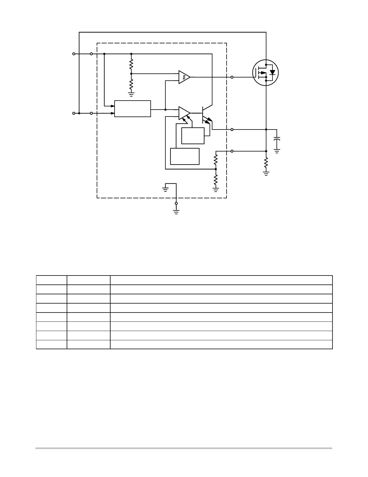
MC33565
5.0 V
Main
Input
1
3.3 V
3
Auxiliary
Input
23.1 k
10.4 k
1.25 V
Reference
Low Voltage
+ Detector
-
4.02 V/
4.17 V
3.3 V
Regulator
+
-
Current
Sense
Thermal
Shutdown 475
289
Switch
Drive
8
G
Regulator
Output
7
6
Sense
Input
D
External
P–Channel
MOSFET
S
3.3 V
+
4.7 mF
Load
Ground 4
Figure 2. Functional Block Diagram
PIN ASSIGNMENTS AND FUNCTIONS
PIN #
FUNCTION
PIN DESCRIPTION
1
Main Input
This input connects to the system main power source, typically 5.0 V.
2, 5
NC
No connection. These pins are not internally connected.
3
Auxiliary Input This input connects to the system auxiliary power source, typically 3.3 V.
4
Gnd
This is the regulator and control circuit power ground.
6
Sense Input
The sense input connects directly to the load allowing precise regulation.
7
Regulator Output This output is precisely regulated at 3.3 V and is capable of up to 200 mA.
8
Switch Drive
This output is designed to drive the gate of an external P–channel MOSFET switch.
http://onsemi.com
2
Share Link: 