MC33348D-3 Просмотр технического описания (PDF) - ON Semiconductor
Номер в каталоге
Компоненты Описание
производитель
MC33348D-3 Datasheet PDF : 15 Pages
| |||
MC33348
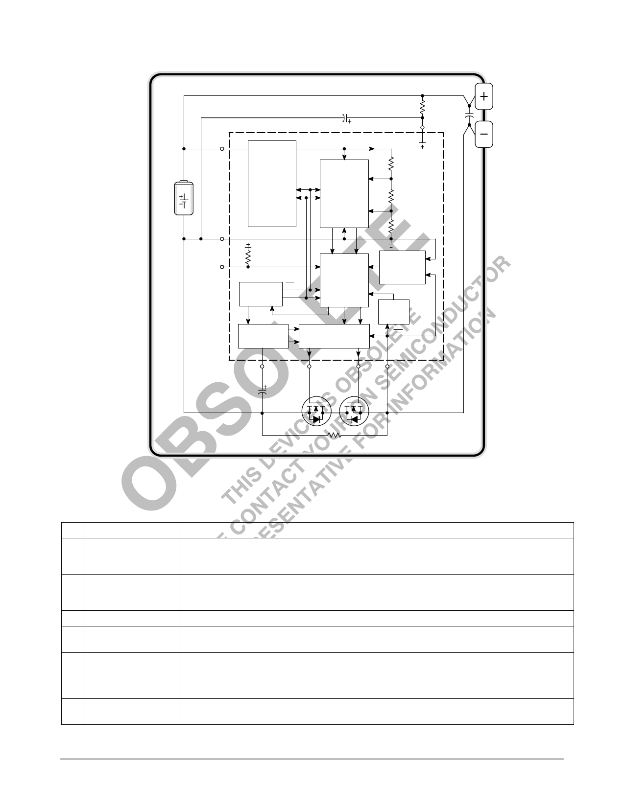
Figure 7. One Cell Smart Battery Pack
10
5.1 k
CI
MC33348
Cell
7 VCC 0.1
Voltage
1
R1
Cell Voltage
Sample
Cell
Switch
Ground
Over/Under
Cell Voltage
Detector
R2
&
Reference
R3
3
Test
2.0 k
2
Ck
Oscillator
Ck
En
Over/Under
Data Latch
&
Control Logic
Discharge
Overcurrent
Detector
Sense
Enable
Charge Pump
Charge/Discharge
Gate Drivers
Charge Pump
Output
CO
0.01
8 Discharge
Gate Drive
Output
Discharge
Switch Q2
4 Charge 6 5 Charge
Gate Drive
Gate Drive
Output
Charge
Switch
Q1
Common/
Discharge
Current Limit
1.0 M
Components CI is mandatory. Refer to the Battery Pack Application text.
PIN FUNCTION DESCRIPTION
Pin
Symbol
ÁÁÁÁÁÁÁÁÁÁÁÁÁÁÁÁÁÁÁÁÁÁÁÁÁÁÁÁÁÁÁÁÁÁ 1 CellVoltage
ÁÁÁÁÁÁÁÁÁÁÁÁÁÁÁÁÁÁÁÁÁÁÁÁÁÁÁÁÁÁÁÁÁÁÁÁÁÁÁÁÁÁÁÁÁÁÁÁÁÁÁÁÁÁÁÁÁÁÁÁÁÁÁÁÁÁÁÁ 2 Test
ÁÁÁÁÁÁÁÁÁÁÁÁÁÁÁÁÁÁÁÁÁÁÁÁÁÁÁÁÁÁÁÁÁÁÁÁÁÁÁÁÁÁÁÁÁÁÁÁÁÁÁÁÁÁÁÁÁÁÁÁÁÁÁÁÁÁÁÁ 3 Ground
ÁÁÁÁÁÁÁÁÁÁÁÁÁÁÁÁÁÁÁÁÁÁÁÁÁÁÁÁÁÁÁÁÁÁ 4 DischargeGateDrive
ÁÁÁÁÁÁÁÁÁÁÁÁÁÁÁÁÁÁÁÁÁÁÁÁÁÁÁÁÁÁÁÁÁÁ Output
ÁÁÁÁÁÁÁÁÁÁÁÁÁÁÁÁÁÁÁÁÁÁÁÁÁÁÁÁÁÁÁÁÁÁ 5 ChargeGateDrive
ÁÁÁÁÁÁÁÁÁÁÁÁÁÁÁÁÁÁÁÁÁÁÁÁÁÁÁÁÁÁÁÁÁÁ Common/Discharge
Current Limit
ÁÁÁÁÁÁÁÁÁÁÁÁÁÁÁÁÁÁÁÁÁÁÁÁÁÁÁÁÁÁÁÁÁÁÁÁÁÁÁÁÁÁÁÁÁÁÁÁÁÁÁÁÁÁÁÁÁÁÁÁÁÁÁÁÁÁÁÁ 6 ChargeGateDrive
ÁÁÁÁÁÁÁÁÁÁÁÁÁÁÁÁÁÁÁÁÁÁÁÁÁÁÁÁÁÁÁÁÁÁÁÁÁÁÁÁÁÁÁÁÁÁÁÁÁÁÁÁÁÁÁÁÁÁÁÁÁÁÁÁÁÁÁÁ Output
Description
This input is connected to the positive terminal of the cell for voltage monitoring. Internally, the Cell
Voltage Sample Switch applies this voltage to a resistor divider where it is compared by the Cell Voltage
Detector to an internal reference.
This pin is normally not connected and is used in testing the protection IC. An active low at this input
resets the internal logic and turns on both MOSFET switches. Upon release, the logic becomes active and
the cell voltage is sampled within 1.0 ms.
This is the protection IC ground and all voltage ratings are with respect to this pin.
This output connects to the gate of discharge switch Q2 allowing it to enable or disable battery pack
discharging.
This is a multifunction pin that is used to monitor cell discharge current and to provide a gate turn−off
path for charge switch Q1. A discharge current limit fault is set when the battery pack load causes the
combined voltage drop of charge switch Q1 and discharge switch Q2 to exceed the discharge current limit
threshold voltage, Vth(dschg), with respect to Pin 3.
This output connects to the gate of charge switch Q1 allowing it to enable or disable battery pack
charging.
http://onsemi.com
6
Share Link: 