MC33348D-1 Просмотр технического описания (PDF) - ON Semiconductor
Номер в каталоге
Компоненты Описание
производитель
MC33348D-1 Datasheet PDF : 15 Pages
| |||
MC33348
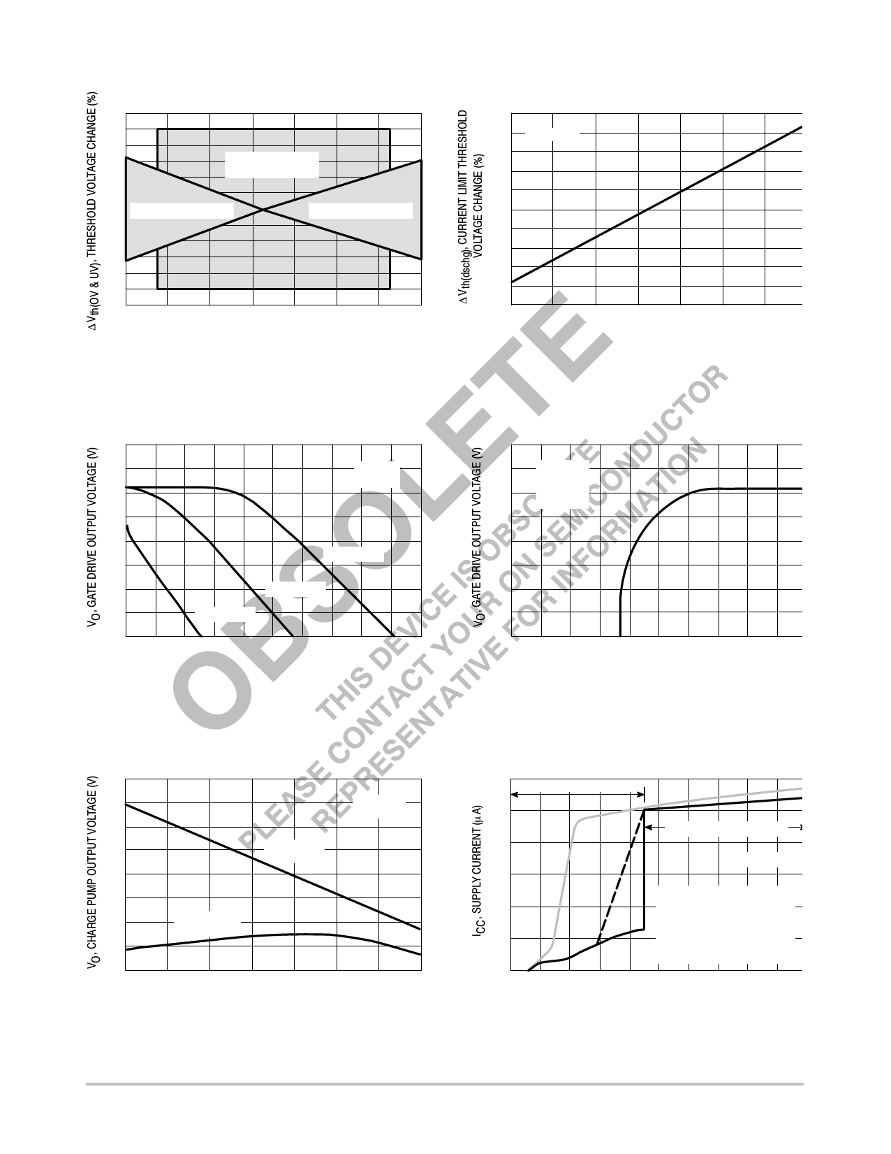
Figure 1. Charge and Discharge
Threshold Voltage Change versus Temperature
1.2
0.8
Maximum Threshold
0.4
Charge Limits
0 Typical Threshold Change
Typical Threshold Change
−0.4
−0.8
−1.2
−40 −20
0
20
40
60
80 100
TA, AMBIENT TEMPERATURE (°C)
Figure 2. Discharge Current Limit
Threshold Voltage Change versus Temperature
16
VCC = 4.0 V
8.0
0
−8.0
−16
−40 −20
0
20
40
60
80 1
TA, AMBIENT TEMPERATURE (°C)
Figure 3. Gate Drive Output Voltage
versus Load Current
12
CO = 10 nF
TA = 25°C
10
8.0
VCC = 4.15 V
6.0
VCC = 3.25 V
VCC = 2.35 V
4.0
0
0.2
0.4
0.6
0.8
1.0
IL, OUTPUT LOAD CURRENT (μA)
Figure 4. Gate Drive Output Voltage
versus Supply Voltage
12
CO = 10 nF
Pin 2 = Gnd
10
RL ≥ 1010 Ω
TA = 25°C
8.0
6.0
4.0
0
1.0
2.0
3.0
4.0
5
VCC, SUPPLY VOLTAGE (V)
Figure 5. Charge Pump Output Voltage
versus Temperature
12
CO = 10 nF
RL ≥ 1010 Ω
11
VCC = 4.15 V
In Regulation
10
9.0
VCC = 2.35 V
Out of Regulation
8.0
−40 −20
0
20
40
60
80 100
TA, AMBIENT TEMPERATURE (°C)
Figure 6. Supply Current
versus Supply Voltage
102
Battery Pack Sleepmode Range
101
100
10−1
10−2
10−3
10−4
0
Battery Pack Operating Range
3
2
1
TA = 25°C
1 − Battery pack unloaded without
discharge current limit fault.
2 − Battery pack loaded without
discharge current limit fault.
3 − Battery pack loaded or unloaded
with discharge current limit fault.
1.0
2.0
3.0
4.0
5
VCC, SUPPLY VOLTAGE (V)
http://onsemi.com
4
Share Link: 