MC100EP16 Просмотр технического описания (PDF) - ON Semiconductor
Номер в каталоге
Компоненты Описание
производитель
MC100EP16 Datasheet PDF : 11 Pages
| |||
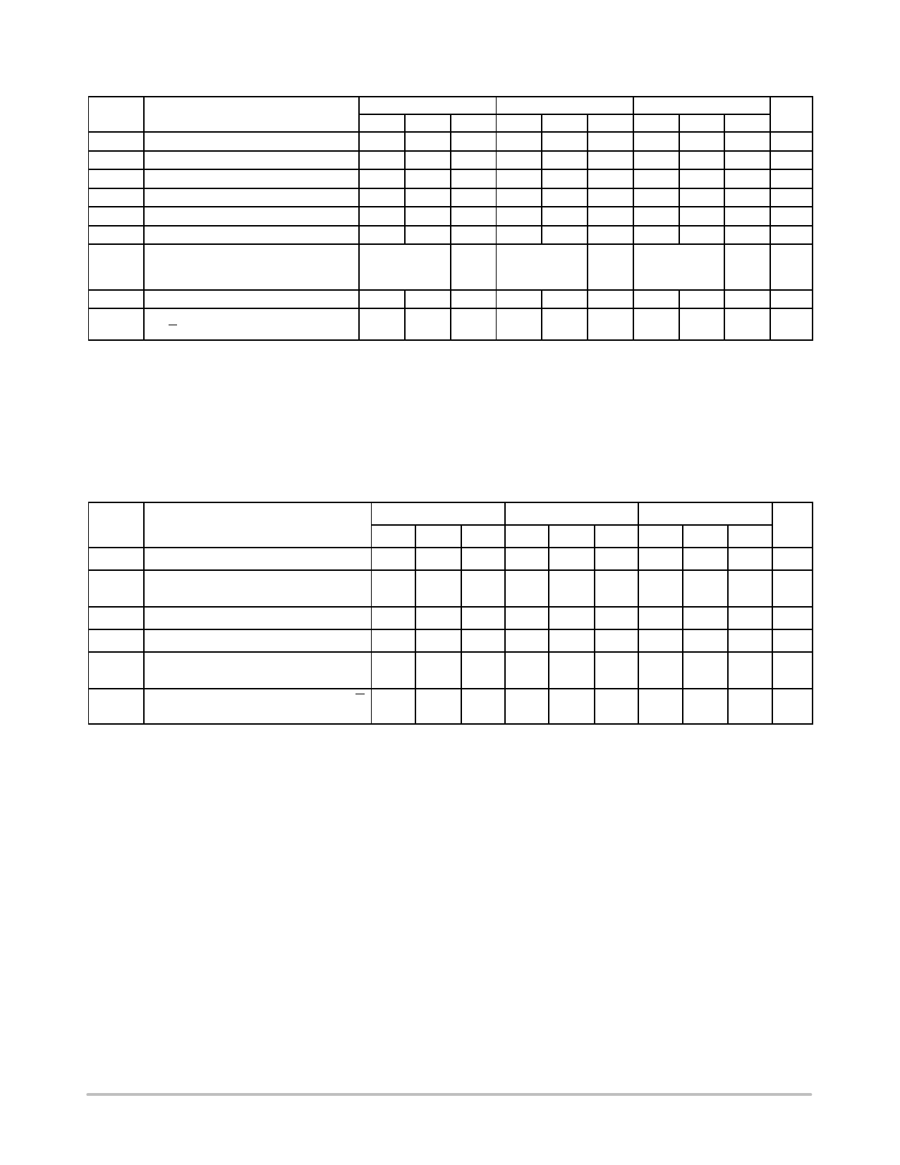
MC10EP16, MC100EP16
Table 9. 100EP DC CHARACTERISTICS, NECL VCC = 0 V; VEE = −5.5 V to −3.0 V (Note 17)
−40°C
25°C
85°C
Symbol
Characteristic
Min Typ Max Min Typ Max Min Typ Max Unit
IEE
VOH
VOL
VIH
VIL
VBB
VIHCMR
Power Supply Current
Output HIGH Voltage (Note 18)
Output LOW Voltage (Note 18)
Input HIGH Voltage (Single−Ended)
Input LOW Voltage (Single−Ended)
Output Voltage Reference
Input HIGH Voltage Common Mode
Range (Differential Configuration)
(Note 19)
17
25
36
17
25
36
22
26
38 mA
−1145 −1020 −895 −1145 −1020 −895 −1145 −1020 −895 mV
−1945 −1820 −1695 −1945 −1820 −1695 −1945 −1820 −1695 mV
−1225
−880 −1225
−880 −1225
−880 mV
−1945
−1625 −1945
−1625 −1945
−1625 mV
−1525 −1425 −1325 −1525 −1425 −1325 −1525 −1425 −1325 mV
VEE + 2.0
0.0
VEE + 2.0
0.0
VEE + 2.0
0.0
V
IIH
Input HIGH Current
IIL
Input LOW Current
D
D 0.5
−150
150
0.5
−150
150
0.5
−150
150 mA
mA
NOTE: Device will meet the specifications after thermal equilibrium has been established when mounted in a test socket or printed circuit
board with maintained transverse airflow greater than 500 lfpm. Electrical parameters are guaranteed only over the declared
operating temperature range. Functional operation of the device exceeding these conditions is not implied. Device specification limit
values are applied individually under normal operating conditions and not valid simultaneously.
17. Input and output parameters vary 1:1 with VCC.
18. All loading with 50 W to VCC −2.0 V.
19. VIHCMR min varies 1:1 with VEE, VIHCMR max varies 1:1 with VCC. The VIHCMR range is referenced to the most positive side of the differential
input signal.
Table 10. AC CHARACTERISTICS VCC = 0 V; VEE = −3.0 V to −5.5 V or VCC = 3.0 V to 5.5 V; VEE = 0 V (Note 20)
−40°C
25°C
85°C
Symbol
Characteristic
Min Typ Max Min Typ Max Min Typ Max Unit
fmax
tPLH,
tPHL
tSKEW
tJITTER
VPP
Maximum Frequency (Figure 2)
Propagation Delay to
Output Differential
Duty Cycle Skew (Note 21)
Cycle−to−Cycle Jitter (Figure 2)
Input Voltage Swing
(Differential Configuration)
>4
>4
>4
GHz
150 220 280 150 220 280 160 240 300 ps
5.0 20
5.0 20
5.0 20 ps
0.2 < 1
0.2 < 1
0.2 < 1 ps
150 800 1200 150 800 1200 150 800 1200 mV
tr
Output Rise/Fall Times
tf
(20% − 80%)
Q, Q 70 120 170 80 130 180 100 150 200 ps
NOTE: Device will meet the specifications after thermal equilibrium has been established when mounted in a test socket or printed circuit
board with maintained transverse airflow greater than 500 lfpm. Electrical parameters are guaranteed only over the declared
operating temperature range. Functional operation of the device exceeding these conditions is not implied. Device specification limit
values are applied individually under normal operating conditions and not valid simultaneously.
20. Measured using a 750 mV source, 50% duty cycle clock source. All loading with 50 W to VCC − 2.0 V.
21. Skew is measured between outputs under identical transitions. Duty cycle skew is defined only for differential operation when the delays
are measured from the cross point of the inputs to the cross point of the outputs.
http://onsemi.com
6
Share Link: 