MC100ELT20DTG(2015) Просмотр технического описания (PDF) - ON Semiconductor
Номер в каталоге
Компоненты Описание
производитель
MC100ELT20DTG Datasheet PDF : 7 Pages
| |||
MC10ELT20, MC100ELT20
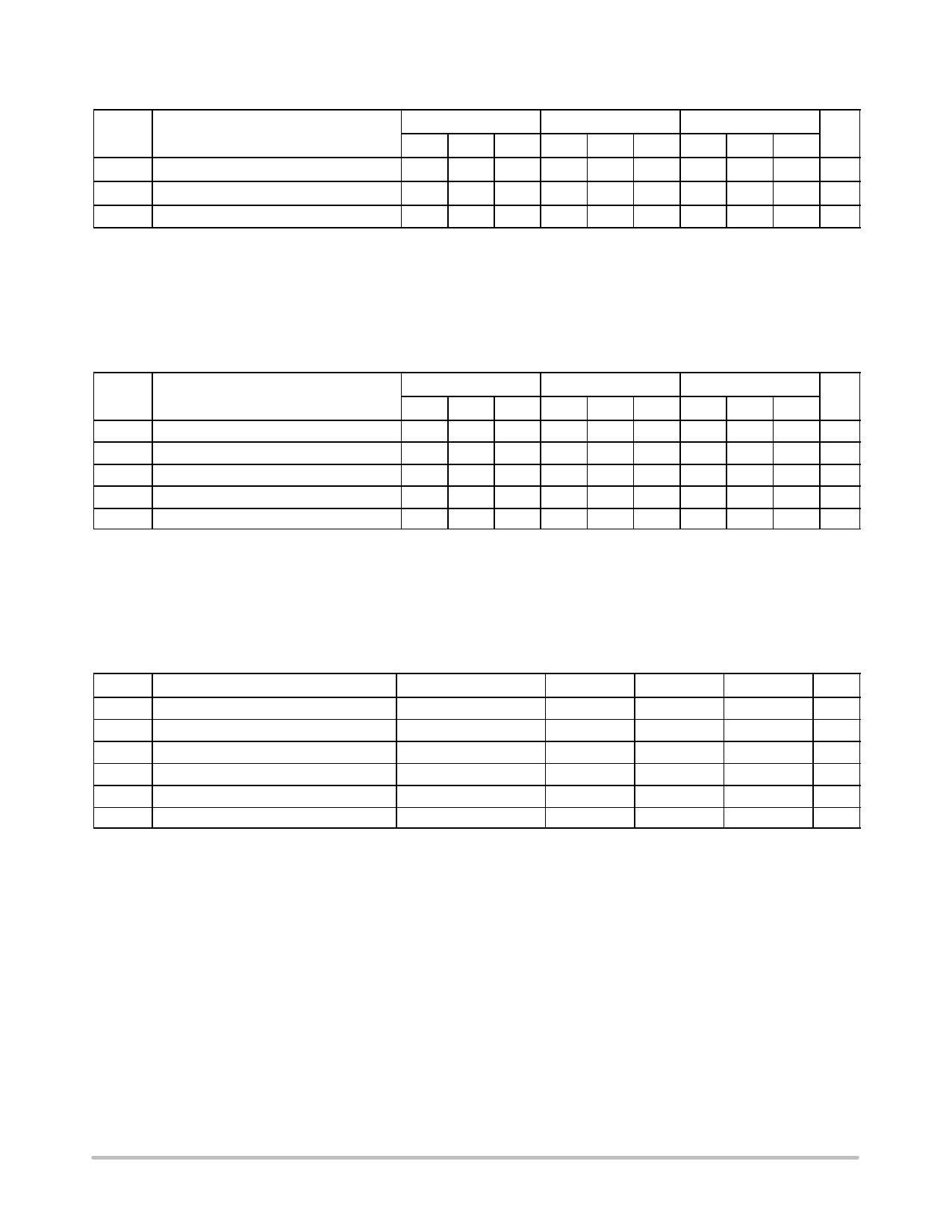
Table 4. 10ELT SERIES PECL DC CHARACTERISTICS VCC = 5.0 V; GND = 0.0 V (Note 2)
−40°C
25°C
85°C
Symbol
Characteristic
ICC
Power Supply Current
VOH
Output HIGH Voltage (Note 3)
VOL
Output LOW Voltage (Note 3)
Min
3920
3050
Typ
4010
3200
Max
16
4110
3350
Min
4020
3050
Typ
4105
3210
Max
16
4190
3370
Min
4090
3050
Typ
4185
3227
Max Unit
16 mA
4280 mV
3405 mV
NOTE: Device will meet the specifications after thermal equilibrium has been established when mounted in a test socket or printed circuit
board with maintained transverse airflow greater than 500 lfpm.
2. Output parameters vary 1:1 with VCC. VCC can vary ±0.25 V.
3. Outputs are terminated through a 50 W resistor to VCC − 2 V.
Table 5. 100ELT SERIES PECL DC CHARACTERISTICS VCC = 5.0 V; GND = 0.0 V (Note 4)
−40°C
25°C
85°C
Symbol
ICC
VOH
VOL
IIH
IIL
Characteristic
Power Supply Current
Output HIGH Voltage (Note 5)
Output LOW Voltage (Note 5)
Input HIGH Current
Input LOW Current
Min
3915
3170
0.5
Typ
3995
3305
Max
16
4120
3445
150
Min
3975
3190
0.5
Typ
4045
3295
Max
16
4120
3380
150
Min
3975
3190
0.5
Typ
4050
3295
Max Unit
16 mA
4120 mV
3380 mV
150 mA
mA
NOTE: Device will meet the specifications after thermal equilibrium has been established when mounted in a test socket or printed circuit
board with maintained transverse airflow greater than 500 lfpm.
4. Output parameters vary 1:1 with VCC. VCC can vary ±0.25 V.
5. Outputs are terminated through a 50 W resistor to VCC − 2 V.
Table 6. TTL INPUT DC CHARACTERISTICS VCC = 4.7 V to 5.27 V; TA = −40°C to 85°C
Symbol
Characteristic
Condition
Min
Typ
Max
Unit
IIH
Input HIGH Current
VIN = 2.7 V
IIHH
Input HIGH Current
VIN = 7.0 V
IIL
Input LOW Current
VIN = 0.5 V
VIK
Input Clamp Diode Voltage
IIN = −18 mA
VIH
Input HIGH Voltage
2.0
VIL
Input LOW Voltage
20
mA
100
mA
−0.6
mA
−1.2
V
V
0.8
V
NOTE: Device will meet the specifications after thermal equilibrium has been established when mounted in a test socket or printed circuit
board with maintained transverse airflow greater than 500 lfpm.
www.onsemi.com
3
Share Link: 