MBM29DL800BA-70 Просмотр технического описания (PDF) - Spansion Inc.
Номер в каталоге
Компоненты Описание
производитель
MBM29DL800BA-70 Datasheet PDF : 57 Pages
| |||
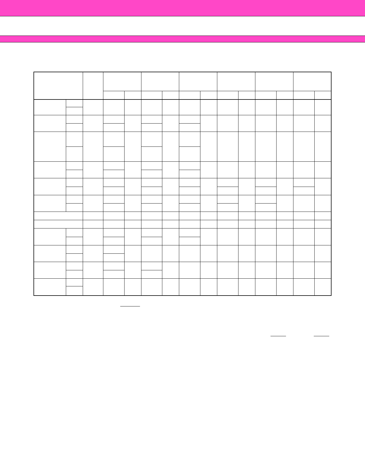
MBM29DL800TA-70/90/MBM29DL800BA-70/90
MBM29DL800TA/BA Command Definitions Table
Command
Sequence
Read/Reset
Read/Reset
Word
Byte
Word
Byte
Autoselect
Word
Byte
Program
Word
Byte
Chip Erase
Word
Byte
Word
Sector Erase
Byte
Erase Suspend
Erase Resume
Set to
Fast Mode
Word
Byte
Fast
Program *1
Word
Byte
Reset from Word
Fast Mode *1 Byte
Extended
Sector
Protect*2
Word
Byte
Bus
Write
Cycles
Req’d
1
3
3
4
6
6
1
1
3
2
2
4
First Bus Second Bus
Write Cycle Write Cycle
Addr. Data Addr. Data
XXXh F0h — —
555h
2AAh
AAh
55h
AAAh
555h
555h
2AAh
AAh
55h
AAAh
555h
555h
2AAh
AAh
55h
AAAh
555h
555h
2AAh
AAh
55h
AAAh
555h
555h
2AAh
AAh
55h
AAAh
555h
BA B0h — —
BA 30h — —
555h
2AAh
AAh
55h
AAAh
555h
XXXh
A0h PA PD
XXXh
BA
BA
90h
XXXh
XXXh
F0h
*3
XXXh 60h SPA 60h
Third Bus
Write Cycle
Addr. Data
——
555h
F0h
AAAh
(BA)
555h
90h
(BA)
AAAh
555h
A0h
AAAh
555h
80h
AAAh
555h
80h
AAAh
——
——
555h
20h
AAAh
——
——
SPA 40h
Fourth Bus
Read/Write
Cycle
Addr. Data
——
RA RD
——
PA PD
555h
AAh
AAAh
555h
AAh
AAAh
——
——
——
——
——
SPA SD
Fifth Bus
Write Cycle
Addr. Data
——
——
——
——
2AAh
55h
555h
2AAh
55h
555h
——
——
——
——
——
——
Sixth Bus
Write Cycle
Addr. Data
——
——
——
——
555h
10h
AAAh
SA 30h
——
——
——
——
——
——
*1 : This command is valid during Fast Mode.
*2 : This command is valid while RESET=VID.
*3 : This data “00h” is also acceptable.
Notes : •Address bits A12 to A18 = X = “H” or “L” for all address commands except or Program Address (PA), Sector
Address (SA), and Bank Address (BA).
• Bus operations are defined in “MBM29DL800TA/BA User Bus Operations Tables (BYTE = VIH and BYTE
= VIL)”.
• RA =Address of the memory location to be read
PA =Address of the memory location to be programmed
Addresses are latched on the falling edge of the write pulse.
SA =Address of the sector to be erased. The combination of A18, A17, A16, A15, A14, A13, and A12 will
uniquely select any sector.
BA =Bank Address (A16 to A18)
• RD =Data read from location RA during read operation.
PD =Data to be programmed at location PA. Data is latched on the rising edge of write pulse.
• SPA =Sector address to be protected. Set sector address (SA) and (A6, A1, A0) = (0, 1, 0).
SD =Sector protection verify data. Output 01h at protected sector addresses and output 00h at
unprotected sector addresses.
• The system should generate the following address patterns:
Word Mode: 555h or 2AAh to addresses A0 to A11
Byte Mode: AAAh or 555h to addresses A–1 and A0 to A11
• Both Read/Reset commands are functionally equivalent, resetting the device to the read mode.
• The command combinations not described in “MBM29DL800TA/BA Command Definitions Table” are illegal.
9
Share Link: 