MAX667(1994) Просмотр технического описания (PDF) - Maxim Integrated
Номер в каталоге
Компоненты Описание
производитель
MAX667 Datasheet PDF : 8 Pages
| |||
+5V/Programmable Low-Dropout
Voltage Regulator
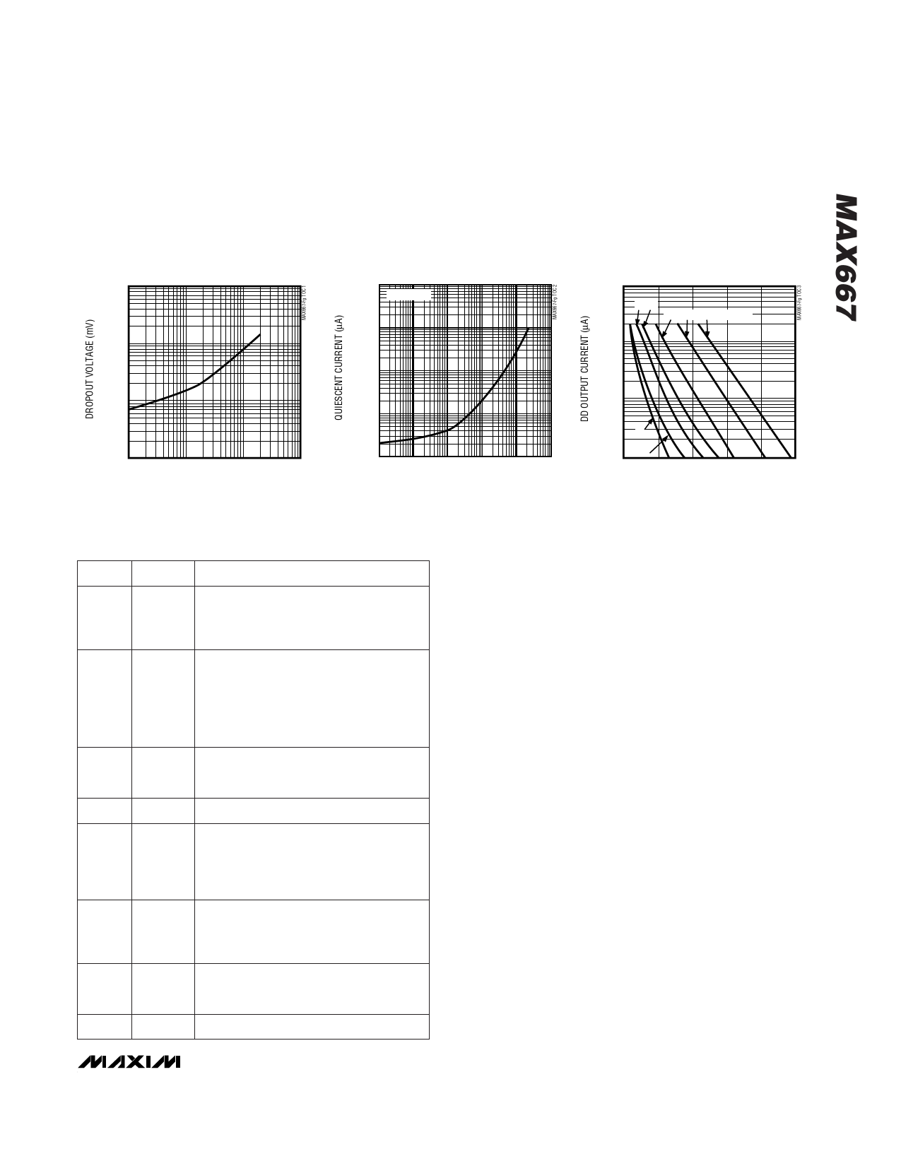
__________________________________________Typical Operating Characteristics
(TA = +25°C, unless otherwise noted.)
1000
100
10
1
1
DROPOUT VOLTAGE
vs. LOAD CURRENT
10
100
LOAD CURRENT (mA)
100,000
QUIESCENT CURRENT
vs. LOAD CURRENT
VIN = +6V
10,000
DD OUTPUT CURRENT
vs. INPUT-OUTPUT DIFFERENCE
1000
5 10
20 50 100mA LOAD
100
1000
1000
100
10
0.01
0.1
1
10 100
LOAD CURRENT (mA)
1000
10
1
1
0
2
50 100 150 200 250
INPUT-OUTPUT DIFFERENCE (mV)
_____________________Pin Description
PIN NAME
FUNCTION
Dropout Detector Output—the collec-
1
DD
tor of a PNP pass transistor. Normally
an open circuit, it sources current as
dropout is reached.
Regulated Output Voltage. OUT falls
to 0V when SHDN is above 1.5V. SET
2
OUT
determines output voltage when SET
is above 50mV; otherwise, it is 5V.
OUT must be connected to an output
filter capacitor.
Low-Battery Detector. A CMOS input
3
LBI
to an internal 1.255V comparator
whose output is the LBO pin.
4
GND Ground
Shutdown Input. Connect to GND for
normal operation (output active). Pull
5
SHDN above 1.5V to disable OUT, LBO, and
DD and to reduce quiescent current to
less than 1µA.
(Output) Voltage Set, CMOS Input.
6
SET
Connect to GND for 5V output. For
other voltages, connect external resis-
tive divider from OUT.
Low-Battery Output. An open-drain N-
7
LBO channel transistor that sinks current to
GND when LBI is less than 1.22V.
8
IN
Positive Input Voltage (unregulated)
_______________Detailed Description
Figure 1 shows a micropower bandgap reference, an
error amplifier, a PNP pass transistor, and two com-
parators as the main elements of the MAX667. One
comparator, C1, selects the fixed 5V or adjustable
operation with an external voltage divider. The other
comparator, C2, is a low-battery detector.
The bandgap reference, which is trimmed to 1.22V,
connects internally to one input of the error amplifier,
A1. The feedback signal from the regulator output sup-
plies the other input of A1 from either an on-chip volt-
age divider or two external resistors. When SET is
grounded, the internal divider provides the error ampli-
fier feedback signal for a fixed 5V output. When SET is
more than 50mV above ground, the error amplifier’s
input switches directly to SET while an external resistor
divider from OUT determines the output voltage.
A second comparator, C2, compares the LBI input to
the internal reference voltage. LBO is an open-drain
FET connected to GND. The low-battery threshold can
also be set with a voltage divider at LBI. In addition, the
MAX667 has a shutdown input (SHDN) that disables
the load and the device while reducing quiescent cur-
rent when it is pulled high.
+5V Output
Figure 2 shows the connection for a fixed 5V output.
The SET input is grounded, and no external resistors
are required. Figure 3 shows adjustable output opera-
tion. R1 and R2 set the output voltage. SHDN should be
grounded if not used.
_______________________________________________________________________________________ 3
Share Link: 