MAX667(1994) Просмотр технического описания (PDF) - Maxim Integrated
Номер в каталоге
Компоненты Описание
производитель
MAX667 Datasheet PDF : 8 Pages
| |||
+5V/Programmable Low-Dropout
Voltage Regulator
ABSOLUTE MAXIMUM RATINGS
Input Supply Voltage ...........................................................+18V
Output Short Circuited to Ground.........................................1sec
LBO Output Sink Current ....................................................50mA
LBO Output Voltage ...............................................GND to VOUT
SHDN Input Voltage ....................................-0.3V to (VIN + 0.3V)
Input Voltages LBI, SET................................-0.3V to (VIN - 1.0V)
Continuous Power Dissipation
Plastic DIP (derate 9.09mW/°C above +70°C) ............727mW
SO (derate 5.88mW/°C above +70°C) .........................471mW
CERDIP (derate 8.00mW/°C above +70°C) .................640mW
Operating Temperature Ranges
MAX667C_A........................................................0°C to +70°C
MAX667E_A .....................................................-40°C to +85°C
MAX667MJA ..................................................-55°C to +125°C
Storage Temperature Range .............................-65°C to +160°C
Lead Temperature (soldering, 10sec) .............................+300°C
Stresses beyond those listed under “Absolute Maximum Ratings” may cause permanent damage to the device. These are stress ratings only, and functional
operation of the device at these or any other conditions beyond those indicated in the operational sections of the specifications is not implied. Exposure to
absolute maximum rating conditions for extended periods may affect device reliability.
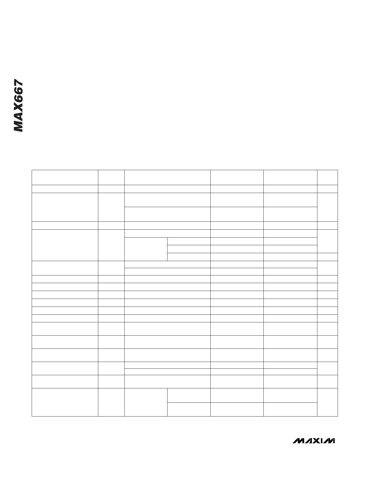
ELECTRICAL CHARACTERISTICS
(GND = 0V, VIN = +9V, VOUT = +5V, C1 = 10µF, unless otherwise noted.)
PARAMETER
SYMBOL
CONDITIONS
TA = +25°C
TA = TMIN to TMAX
MIN TYP MAX MIN TYP MAX
UNITS
Input Voltage
Output Voltage
VIN
VOUT
VSET = 0V, VIN = 6V, IOUT = 10mA,
TA = -40°C to +85°C
VSET = 0V, VIN = 6V, IOUT = 10mA,
TA = -55°C to +125°C
3.5
16.5
V
5
4.8
5.2
V
5
4.75
5.25
Maximum Output Current
Quiescent Current
Dropout Voltage (Note1)
Load Regulation
Line Regulation
SET Reference Voltage
SET Input Leakage Current
Output Leakage Current
Short-Circuit Current
Low-Battery Detector
Reference Voltage
Low-Battery Detector
Input Leakage Current
Low-Battery Detector
Output Voltage
SHDN Threshold
IOUT
IQ
VSET
ISET
IOUT
IOUT
VLBI
VIN = 6V, 4.5V < VOUT < 5.5V
250
VSHDN = 2V
VSHDN = 0V,
VSET = 0V
IOUT = 0µA
IOUT = 100µA
IOUT = 200mA
IOUT = 100µA
IOUT = 200mA
IOUT = 10mA to 200mA
VIN = 6V to 10V, IOUT = 10mA
VSET = 1.5V
VSHDN = 2V
(Note 2)
ILBI
VLBI = 1.5V
VLBO VIN = 9V, VLBI = 2V, ILBO = 10mA
VSHDN
VIH
VIL
1.5
250
0.2 1
20 25
20 30
5 15
5 60
150 250
50 100
5 10
1.225
1.20
0.01 ±10
0.1
400
1.225
1.195
0.01 ±10
0.25
1.5
0.3
mA
2
35
µA
50
20
mA
75
mV
350
250 mV
15
mV
1.25
V
±1000 nA
1
µA
450 mA
1.255 V
±1000 nA
0.4
V
0.3
V
SHDN Leakage Current
ISHDN VSHDN = 0V to VIN
0.01 ±10
±1000 nA
Dropout Detector Output
Voltage
VDD
VSET = 0V,
VSHDN = 0V,
RDD = 100kΩ,
IOUT = 10mA
VIN = 7V
VIN = 4.5V
0.25
V
3.5
Note 1: Dropout Voltage is VIN-VOUT when VOUT falls to 0.1V below its value at VIN = VOUT + 2V.
Note 2: Short-Circuit Current is pulse tested to maintain junction temperature. Short-circuit duration is limited by package dissipation.
2 _______________________________________________________________________________________
Share Link: 