MAX4699 Просмотр технического описания (PDF) - Maxim Integrated
Номер в каталоге
Компоненты Описание
производитель
MAX4699 Datasheet PDF : 11 Pages
| |||
Low-Voltage, Dual DPDT/Quad SPDT
Analog Switches in QFN
Power-Supply Sequencing and
Overvoltage Protection
Caution: Do not exceed the absolute maximum rat-
ings because stresses beyond the listed ratings
may cause permanent damage to the devices.
Proper power-supply sequencing is recommended for
all CMOS devices. Always apply V+ before applying
analog signals, especially if the analog signal is not cur-
rent limited. If this sequencing is not possible, and if the
analog inputs are not current limited to <20mA, add a
small-signal diode (D1) as shown in Figure 1. If the ana-
log signal can dip below GND, add D2. Adding protec-
tion diodes reduces the analog range to a diode drop
(about 0.7V) below V+ (for D1), and a diode drop above
ground (for D2). On-resistance increases slightly at low
supply voltages. Maximum supply voltage (V+) must not
exceed +6V.
Adding protection diode D2 causes the logic threshold
to be shifted relative to GND. TTL compatibility is not
guaranteed when D2 is added.
Protection diodes D1 and D2 also protect against some
overvoltage situations. With Figure 1’s circuit, if the sup-
ply voltage is below the absolute maximum rating, and
if a fault voltage up to the absolute maximum rating is
applied to an analog signal pin, no damage will result.
VL Logic Input (MAX4702)
The MAX4702 features a VL logic input that allows for
lower logic input thresholds down to 1.0V min for VIH in
the quad SPDT configuration. Power-up VL after V+ has
been powered with a minimum of 1.5V to ensure proper
operation of the device.
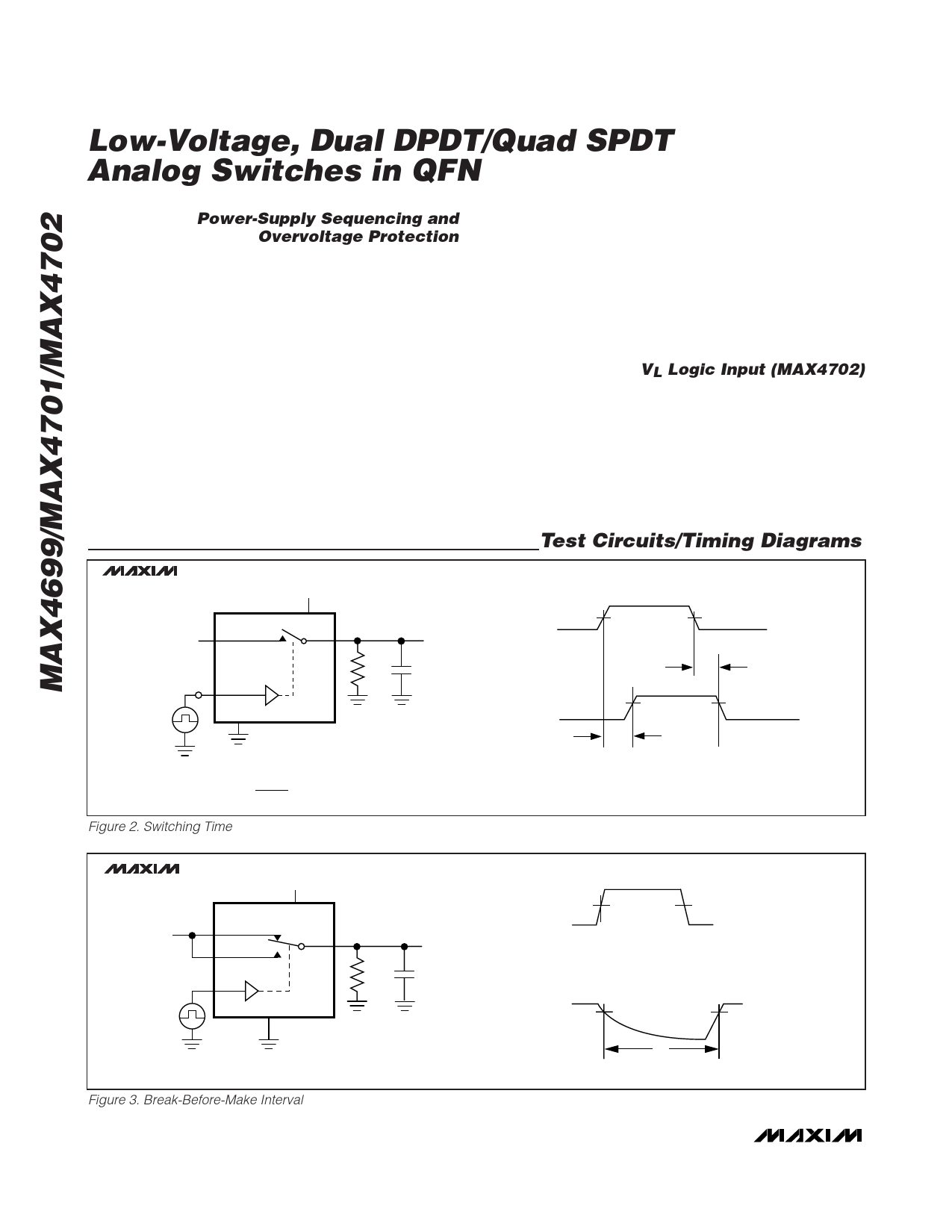
Test Circuits/Timing Diagrams
MAX4699
MAX4701
MAX4702
VN_
NO_
OR NC_
LOGIC
INPUT
IN_
GND
V+
V+
COM_
RL
300Ω
VOUT
CL
35pF
CL INCLUDES FIXTURE AND STRAY CAPACITANCE.
( ) VOUT = VN_
RL
RL + RON
Figure 2. Switching Time
LOGIC VIH
INPUT VIL
50%
tr < 5ns
tf < 5ns
SWITCH 0
OUTPUT
tOFF
VOUT 0.9 x V0UT
0.9 x VOUT
tON
LOGIC INPUT WAVEFORMS INVERTED FOR SWITCHES
THAT HAVE THE OPPOSITE LOGIC SENSE.
MAX4699
MAX4701
MAX4702
VN_
LOGIC
INPUT
V+
V+
NC_
COM_
NO_
IN_
GND
VOUT
RL
300Ω
CL
35pF
CL INCLUDES FIXTURE AND STRAY CAPACITANCE.
Figure 3. Break-Before-Make Interval
LOGIC VIH
INPUT
50%
VIL
VOUT
0.9 x VOUT
tD
8 _______________________________________________________________________________________
Share Link: 