MAX4670 Просмотр технического описания (PDF) - Maxim Integrated
Номер в каталоге
Компоненты Описание
производитель
MAX4670 Datasheet PDF : 20 Pages
| |||
Integrated T1/E1/J1 Short-Haul and
Long-Haul Protection Switch
ABSOLUTE MAXIMUM RATINGS
(All voltages referenced to GND.)
V+, IN_, SWITCH ......................................................-0.3V to +4V
COM_, NO_, NC_ (Note 1) ...........................-0.3V to (V+ + 0.3V)
Continuous Current
NO_, NC_, COM_ (Tx interface)..................................±150mA
NO_, NC_, COM_ (Rx interface) .................................±100mA
Peak Currents
NO_, NC_, COM_ (Tx interface)
(pulsed at 1ms, 10% duty cycle) ................................±300mA
NO_, NC_, COM_ (Rx interface)
(pulsed at 1ms, 10% duty cycle) ................................±200mA
Peak Surge Currents
Poised at 8µs ..................................................................21.4A
Poised at 20µs ................................................................11.9A
Continuous Power Dissipation (TA = +70°C)
32-Pin TQFN (derate 21.3mW/°C above +70°C) .......1702mW
38-Pin TSSOP (derate 13.7mW/°C above +70°C) .....1096mW
Operating Temperature Range ...........................-40°C to +85°C
Storage Temperature Range .............................-65°C to +150°C
Junction Temperature ......................................................+150°C
Lead Temperature (soldering, 10s) .................................+300°C
Note 1: Signals on NO_, NC_, COM_ exceeding V+ or GND are clamped by internal diodes. Limit forward-diode current to maximum
current rating.
Stresses beyond those listed under “Absolute Maximum Ratings” may cause permanent damage to the device. These are stress ratings only, and functional
operation of the device at these or any other conditions beyond those indicated in the operational sections of the specifications is not implied. Exposure to
absolute maximum rating conditions for extended periods may affect device reliability.
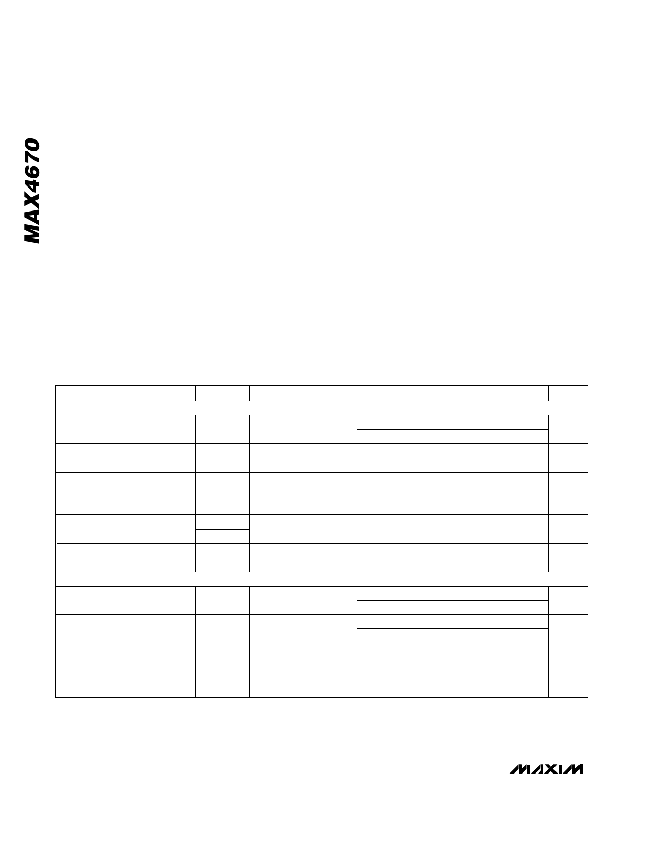
ELECTRICAL CHARACTERISTICS
(V+ = +2.7V to +3.6V, TA = TMIN to TMAX, unless otherwise noted. Typical values are at TA = +25°C, unless otherwise noted.) (Notes 2, 3)
PARAMETER
Rx INTERFACE
On-Resistance
On-Resistance Match Between
Channels (Note 4)
SYMBOL
CONDITIONS
MIN TYP MAX UNITS
RON
∆RON
V+ = 3V, ICOM_ = 10mA,
VNO_ or VNC_ = 1.5V
V+ = 3V, ICOM_ = 10mA,
VNO_ or VNC_ = 1.5V
TA = +25°C
TA = TMIN to TMAX
TA = +25°C
TA = TMIN to TMAX
5
9
Ω
10
1.0
Ω
1.3
On-Resistance Flatness (Note 4)
RFLAT(ON)
V+ = 3V; ICOM_ = 10mA;
VNO_ or VNC_ = 1.0V,
1.5V, 2.0V
TA = +25°C
TA = TMIN to TMAX
2.0
3.0
Ω
3.4
NO_ or NC_ Off-Leakage
Current
COM_ On-Leakage Current
Tx INTERFACE
On-Resistance (Note 5)
On-Resistance Match Between
Channels (Notes 3, 5)
INO(OFF) V+ = 3.6V; VCOM_ = 0.3V, 3.3V;
INC (OFF) VNO_ or VNC_ = 3.3V, 0.3V
-1
ICOM(ON)
V+ = 3.6V; VCOM_ = 0.3V, 3.3V;
VNO_ or VNC_ = 3.3V, 0.3V or floating
-1
RON
∆RON
V+ = 3V, ICOM_ = 100mA,
VNO_ or VNC_ = 1.5V
V+ = 3V, ICOM_ = 100mA,
VNO_ or VNC_ = 1.5V
TA = +25°C
TA = TMIN to TMAX
TA = +25°C
TA = TMIN to TMAX
+1
µA
+1
µA
0.7
0.9
Ω
1.0
0.03 0.150
Ω
0.175
On-Resistance Flatness
(Notes 5, 6)
RFLAT(ON)
V+ = 3V;
ICOM_ = 100mA;
VNO_ or VNC_ = 1.0V,
1.5V, 2.0V
TA = +25°C
TA = TMIN to TMAX
0.1 0.18
Ω
0.2
2 _______________________________________________________________________________________
Share Link: 