MAX3625B Просмотр технического описания (PDF) - Maxim Integrated
Номер в каталоге
Компоненты Описание
производитель
MAX3625B Datasheet PDF : 10 Pages
| |||
Low-Jitter, Precision Clock
Generator with Three Outputs
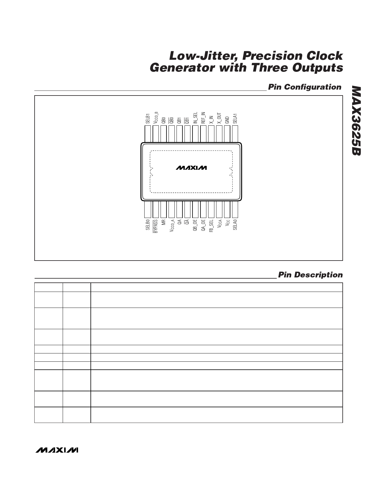
Pin Configuration
TOP VIEW
24 23 22 21 20 19 18 17 16 15 14 13
MAX3625B
*EP
+
1 2 3 4 5 6 7 8 9 10 11 12
TSSOP
*EXPOSED PAD MUST BE SOLDERED TO GROUND FOR PROPER
THERMAL AND ELECTRICAL OPERATION.
PIN
1, 24
2
3
4
5
6
7
8
9
Pin Description
NAME
SELB0,
SELB1
BYPASS
MR
VCCO_A
QA
QA
QB_OE
QA_OE
FB_SEL
FUNCTION
LVCMOS/LVTTL Inputs. Control NB divider setting. Has 50k input impedance. See Table 2 for more
information.
LVCMOS/LVTTL Input (Active Low). Connect low to bypass the internal PLL. Connect high or leave
open for normal operation. When in bypass mode the output dividers are set to divide by 1. Has
internal 75k pullup to VCC.
LVCMOS/LVTTL Input. Master reset input. Pulse high for > 1μs to reset all dividers. Has internal 75k
pulldown to GND. Not required for normal operation.
Power Supply for QA Clock Output. Connect to +3.3V.
Noninverting Clock Output, LVPECL
Inverting Clock Output, LVPECL
LVCMOS/LVTTL Input. Enables/disables QB clock outputs. Connect pin high or leave open to enable
LVPECL clock outputs QB0 and QB1. Connect low to set QB0 and QB1 to a logic 0. Has internal 75k
pullup to VCC.
LVCMOS/LVTTL Input. Enables/disables the QA clock output. Connect high or leave open to enable the
LVPECL clock output QA. Connect low to set QA to a logic 0. Has internal 75k pullup to VCC.
LVCMOS/LVTTL Input. Controls M divider setting. See Table 3 for more information. Has internal 75k
pulldown to GND.
_______________________________________________________________________________________ 5
Share Link: 