MAX3629 Просмотр технического описания (PDF) - Maxim Integrated
Номер в каталоге
Компоненты Описание
производитель
MAX3629 Datasheet PDF : 12 Pages
| |||
+3.3V, Low-Jitter, Precision Clock Generator
with Multiple Outputs
Detailed Description
The MAX3629 is a frequency generator designed to
operate at Ethernet frequencies. It consists of an on-
chip crystal oscillator, PLL, LVCMOS output buffers,
and LVDS output buffers. Using a low-frequency clock
(crystal or CMOS input) as a reference, the internal PLL
generates a high-frequency output clock with excellent
jitter performance. The outputs can be switched among
125MHz, 156.25MHz, and 312.5MHz.
Crystal Oscillator
An integrated oscillator provides the low-frequency ref-
erence clock for the PLL. This oscillator requires an
external crystal connected between X_IN and X_OUT.
The crystal frequency is 25MHz.
OSC_IN Buffer
The LVCMOS OSC_IN buffer is internally biased to
allow AC- or DC-coupling. This input is internally AC-
coupled, and is designed to operate at 25MHz when
the PLL is enabled (PLL_BP is left open). When the PLL
is bypassed (PLL_BP is set low), the OSC_IN buffer can
be operated from 20MHz to 320MHz.
PLL
The PLL takes the signal from the crystal oscillator or
reference clock input and synthesizes a low-jitter, high-
frequency clock. The PLL contains a phase-frequency
detector (PFD), a lowpass filter, and a voltage-con-
trolled oscillator (VCO) that operates at 625MHz. The
VCO output is connected to the PFD input through a
feedback divider that divides the VCO frequency by 25
to lock onto the 25MHz reference clock or oscillator. For
output Q0, the FSELA pin is used to select among
125MHz, 156.25MHz, and 312.5MHz. For outputs Q1 to
Q4, the FSELB pin is used to select among 125MHz,
156.25MHz, and 312.5MHz. For outputs Q5, Q6, and
Q7, the FSELB pin is used to select between 125MHz
and 156.25MHz. To minimize noise-induced jitter, the
VCO supply (VDDA) is isolated from the core logic and
output buffer supplies.
LVDS Drivers
The high-frequency outputs—Q0, Q1, Q2, Q3, and Q4—
are differential LVDS buffers designed to drive 100Ω.
LVCMOS Driver
LVCMOS outputs Q5, Q6, and Q7 are provided on the
MAX3629. They are designed to drive single-ended
high-impedance loads. The output specifications are
only valid up to 160MHz.
Applications Information
Power-Supply Filtering
The MAX3629 is a mixed analog/digital IC. The PLL
contains analog circuitry susceptible to random noise.
To take full advantage of on-board filtering and noise
attenuation, in addition to excellent on-chip power-sup-
ply rejection, this part provides a separate power-sup-
ply pin, VDDA, for the VCO circuitry. The purpose of this
design technique is to ensure clean input power supply
to the VCO circuitry and to improve the overall immunity
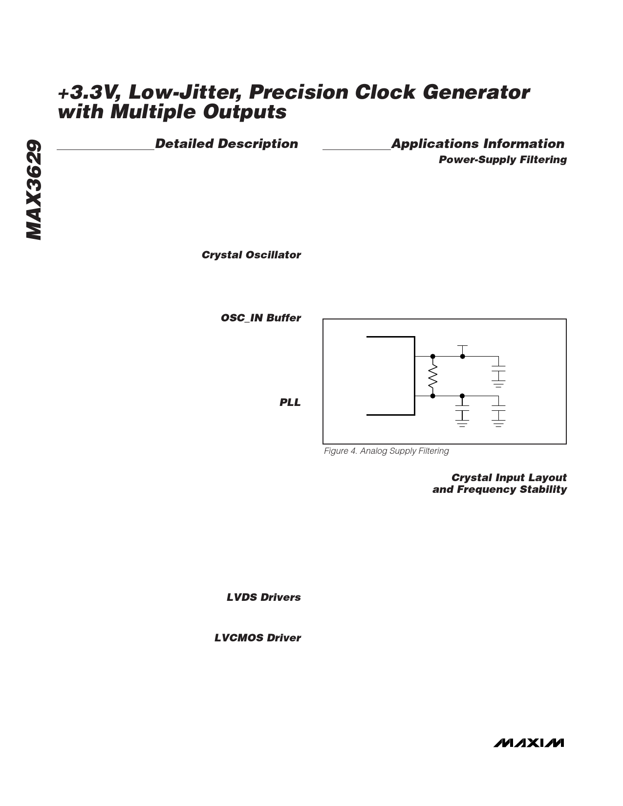
to power-supply noise. Figure 4 illustrates the recom-
mended power-supply filter network for VDDA. This net-
work requires that the power supply is +3.3V ±5%.
Decoupling capacitors should be used on all other sup-
ply pins for best performance.
+3.3V ±5%
VDD
10.5Ω
0.1μF
VDDA
0.01μF 10μF
Figure 4. Analog Supply Filtering
Crystal Input Layout
and Frequency Stability
The MAX3629 features integrated on-chip crystal oscil-
lators to minimize system implementation cost. The inte-
grated crystal oscillator is a Pierce-type that uses the
crystal in its parallel resonance mode. It is recommend-
ed to use a 25MHz crystal with a load specification of
CL = 18pF. The crystal frequency should be chosen so
that the VCO operates at 625MHz. See Table 1 for the
recommended crystal specifications.
The crystal, trace, and two external capacitors should
be placed on the board as close as possible to the
X_IN and X_OUT pins to reduce crosstalk and active
signals into the oscillator.
The layout shown in Figure 5 gives approximately 2pF
of trace plus footprint capacitors per side of the crystal
(Y1). The dielectric material is FR-4 and dielectric thick-
ness of the reference board is 15 mils. Using a 25MHz
crystal and the capacitor values of C45 = 27pF and
10 ______________________________________________________________________________________
Share Link: 