MAX3672 Просмотр технического описания (PDF) - Maxim Integrated
Номер в каталоге
Компоненты Описание
производитель
MAX3672 Datasheet PDF : 12 Pages
| |||
Low-Jitter 155MHz/622MHz Clock Generator
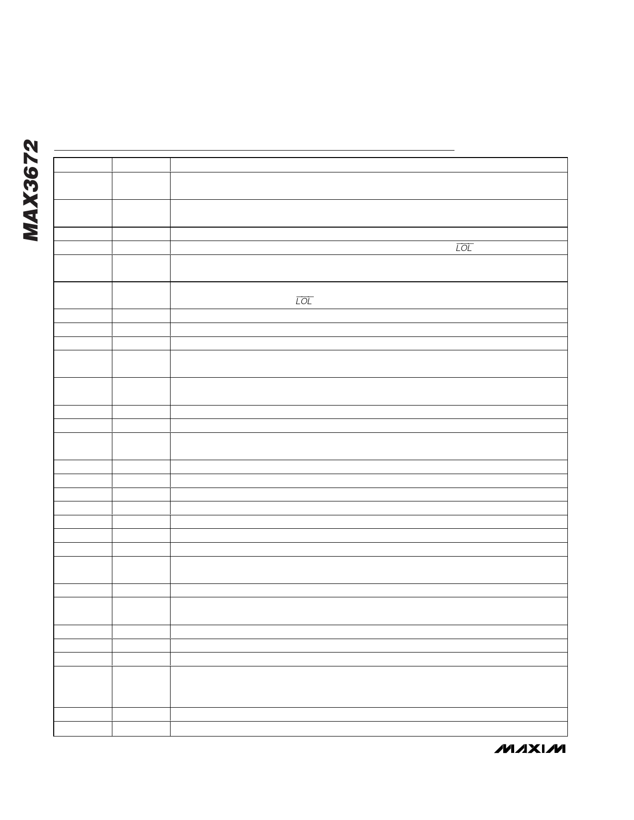
Pad Description
PAD
1
2
3, 10, 16
4
5, 12, 18, 27,
33
6
7
8
9
11
13
14
15
17
19
20
21, 24
22
23
25
26
28
29
30
31
32
34
35
36
37
NAME
C2+
C2-
VCCD
THADJ
GND
CTH
NSEL1
NSEL2
GSEL
LOL
RSEL
REFCLK+
REFCLK-
VSEL
POUT-
POUT+
VCCO
MOUT-
MOUT+
VCOIN-
VCOIN+
VFILTER
VC
POLAR
PSEL1
PSEL2
VCCA
COMP
OPAMP-
OPAMP+
FUNCTION
Positive Filter Input. External capacitor connected between C2+ and C2- used for setting the higher
order pole frequency (see the Setting the Higher-Order Poles section).
Negative Filter Input. External capacitor connected between C2+ and C2- used for setting the higher
order pole frequency (see the Setting the Higher-Order Poles section).
Positive Digital Supply Voltage
Threshold Adjust Input. Used to adjust the loss-of-lock threshold (see the LOL Setup section).
Ground
Threshold Capacitor Input. Connect capacitor connected between CTH and ground to control the
loss-of-lock conditions (see the LOL Setup section).
Divide Selector 1 Input. Three-level pin used to set the frequency divider ratio (N2) (Table 3).
Divide Selector 2 Input. Three-level pin used to set the frequency divider ratio (N2) (Table 3).
Gain Selector Input. Three-level pin used to set the phase-detector gain (Kpd) (Table 4).
Loss of Lock. LOL signals a TTL low when the reference frequency differs from the VCO frequency.
LOL signals a TTL high when the reference frequency equals the VCO frequency.
Reference Clock Selector Input. Three-level pin used to set the pre-divider ratio (N3) for the input
reference clock (Table 1).
Positive Reference Clock Input, PECL
Negative Reference Clock Input, PECL
VCO Clock Selector Input. Three-level pin used to set the pre-divider ratio (N1) for the input VCO
clock (Table 2).
Negative Optional Clock Output, PECL
Positive Optional Clock Output, PECL
Positive Supply Voltage for PECL Outputs
Negative Main Clock Output, PECL
Positive Main Clock Output, PECL
Negative VCO Clock Input, PECL
Positive VCO Clock Input, PECL
Optional Noise Filter. Connect an external capacitor to reduce PECL output noise (see the Typical
Application Circuit).
Control Voltage Output. The voltage output from the op amp that controls the VCO.
Polarity Control of Op Amp Input. POLAR = GND for VCOs with positive-gain transfer. POLAR = VCC
for VCOs with negative-gain transfer.
Optional Clock Selector 1 Input. Sets the divider ratio for the optional clock output (Table 5).
Optional Clock Selector 2 Input. Sets the divider ratio for the optional clock output (Table 5).
Positive Analog Supply Voltage for the Charge Pump and Op Amp
Compensation Control Input. Op Amp Compensation Reference Control Input. COMP = GND for
VCOs whose control pin is VCC referenced. COMP = VCC for VCOs whose control pin is GND
referenced.
Negative Op Amp Input, POLAR = GND
Positive Op Amp Input, POLAR = GND
6 _______________________________________________________________________________________
Share Link: 