MAX3670 Просмотр технического описания (PDF) - Maxim Integrated
Номер в каталоге
Компоненты Описание
производитель
MAX3670 Datasheet PDF : 12 Pages
| |||

Low-Jitter 155MHz/622MHz
Clock Generator
Depending on the input clock frequency of 77.76MHz,
155.52MHz, or 622.08MHz, the clock divider ratio must
be set to 1, 2, or 8, respectively. The POUT output
buffer is preceded by a clock divider that scales the
main clock output by 1, 2, 4, or 8 to provide an optional
clock.
LOL Detection Circuitry
The MAX3670 incorporates a loss-of-lock (LOL) monitor
that consists of an XOR gate, filter, and comparator
with adjustable threshold (see “LOL Setup” in the
Applications section). A loss-of-lock condition is sig-
naled with a TTL low when the reference clock frequen-
cy differs from the VCO frequency.
Gain-Control Logic
The gain-control circuitry facilitates the tuning of the
loop bandwidth by setting phase-detector gain and fre-
quency-divider ratio. The gain-control logic can be pro-
grammed to divide from 1 to 1024, in binary multiples,
and to adjust the phase detector gain to 5µA/UI or
20µA/UI (see Table 3 in Setting the Loop Bandwidth
section).
Phase-Frequency Detector and
Charge Pump
The phase-frequency detector incorporated into the
MAX3670 produces pulses proportional to the phase
difference between the reference clock and the VCO
input. The charge pump converts this pulse train to a
current signal that is fed to the op amp.
Op Amp
The op amp is used to form an active PLL loop filter
capable of driving the VCO control voltage input. Using
the POLAR input, the op amp input polarity can be select-
ed to work with VCOs having positive or negative gain-
transfer functions. The COMP pin selects the op amp
internal compensation. Connect COMP to ground if the
VCO control voltage is VCC referenced. Connect COMP
to VCC if the VCO control voltage is ground referenced.
Design Procedure
Setting Up the VCO and
Reference Clock
The MAX3670 accepts 77.76MHz, 155.52MHz, or
622.08MHz (including FEC rates) reference clock fre-
quencies. The RSEL input must be set so that the refer-
ence clock is prescaled to 77.76MHz (or FEC rate), to
provide the proper range for the PFD and LOL detec-
tion circuitry. Table 1 shows the divider ratio for the dif-
ferent reference frequencies.
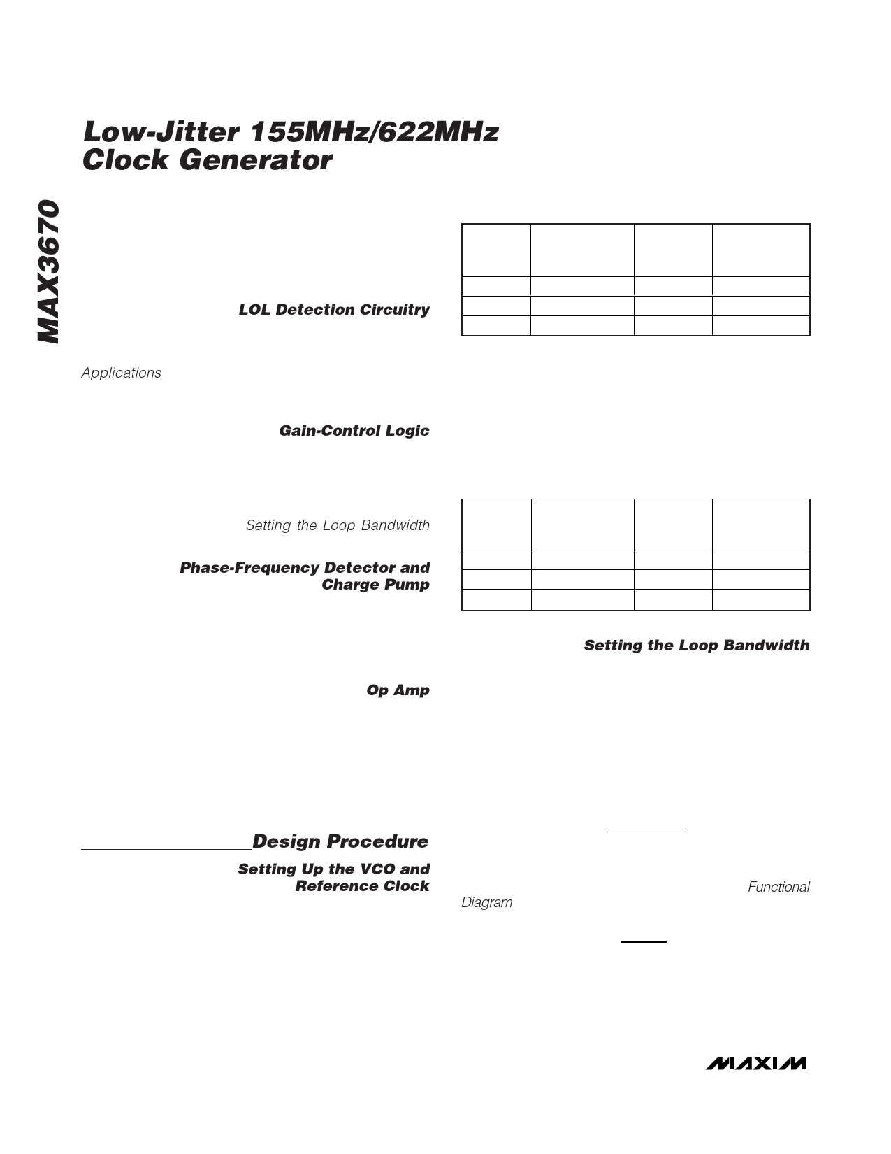
Table 1. Reference Clock Divider
INPUT
PIN
RSEL
VCC
OPEN
GND
REFERENCE
CLOCK INPUT
FREQ. (MHz)
77.76
155.52
622.08
DIVIDER
RATIO N3
1
2
8
PREDIVIDER
OUTPUT
FREQ. (MHz)
77.76
77.76
77.76
The MAX3670 is designed to accept 77.76MHz,
155.52MHz, or 622.08MHz (including FEC rates) volt-
age-controlled oscillator (VCO) frequencies. The VSEL
input must be set so that the VCO input is prescaled to
77.76MHz (or FEC rate), to provide the proper range for
the PFD and LOL detection circuitry. Table 2 shows the
divider ratio for the different VCO frequencies.
Table 2. VCO Clock Divider
INPUT
PIN
VSEL
VCC
OPEN
GND
VCO CLOCK
INPUT FREQ.
(MHz)
77.76
155.52
622.08
DIVIDER
RATIO N1
1
2
8
PREDIVIDER
OUTPUT
FREQ. (MHz)
77.76
77.76
77.76
Setting the Loop Bandwidth
To eliminate jitter present on the reference clock, the
proper selection of loop bandwidth is critical. If the total
output jitter is dominated by the noise at the reference
clock input, then lowering the loop bandwidth will
reduce system jitter. The loop bandwidth (K) is a func-
tion of the VCO gain (KVCO), the gain of the phase
detector (KPD), the loop filter resistor (R1), and the total
feedback-divider ratio (N = N1 ✕ N2). The loop band-
width of the MAX3670 can be approximated by
K = KPDR1KVCO
2πN
For stability, a zero must be added to the loop in the form
of resistor R1 in series with capacitor C1 (see Functional
Diagram). The location of the zero can be approximated as
fZ
=
1
2πR1C1
Due to the second-order nature of the PLL jitter trans-
fer, peaking will occur and is proportional to fZ/K. For
certain applications, it may be desirable to limit jitter
8 _______________________________________________________________________________________